Nitride semiconductor laser device and a method for improving its performance

Inactive Publication Date: 2008-01-01
AMMONO SP Z O O (PL)
View PDF9 Cites 10 Cited by
  • Summary
  • Abstract
  • Description
  • Claims
  • Application Information

AI Technical Summary

Benefits of technology

[0031]In the method for improving the performance of a nitride semiconductor laser device according to the present invention the resonator end face window layer is formed by deposit

Problems solved by technology

In nitride semiconductor lasers, resonator mirrors are obtained as a result of Reactive Ion Etching (RIE) or cleavage, and—due to energy gap narrowing—they absorb emitted radiation, which results in heat generation leading to impairment of the lifetime of over 100 mW laser diodes.
However, such high tem

Method used


Image

  • Nitride semiconductor laser device and a method for improving its performance
  • Nitride semiconductor laser device and a method for improving its performance
  • Nitride semiconductor laser device and a method for improving its performance

Examples


example 1

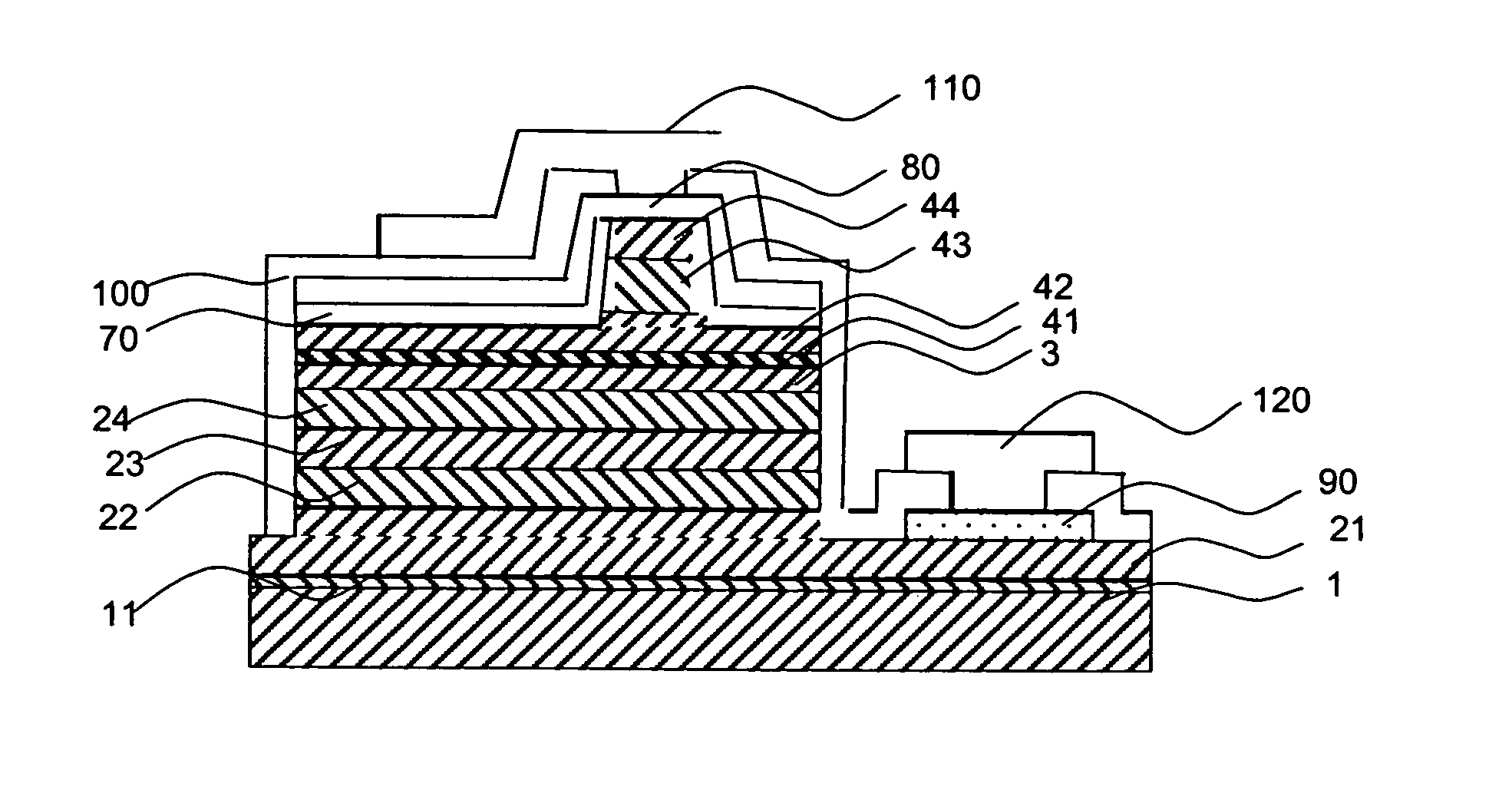
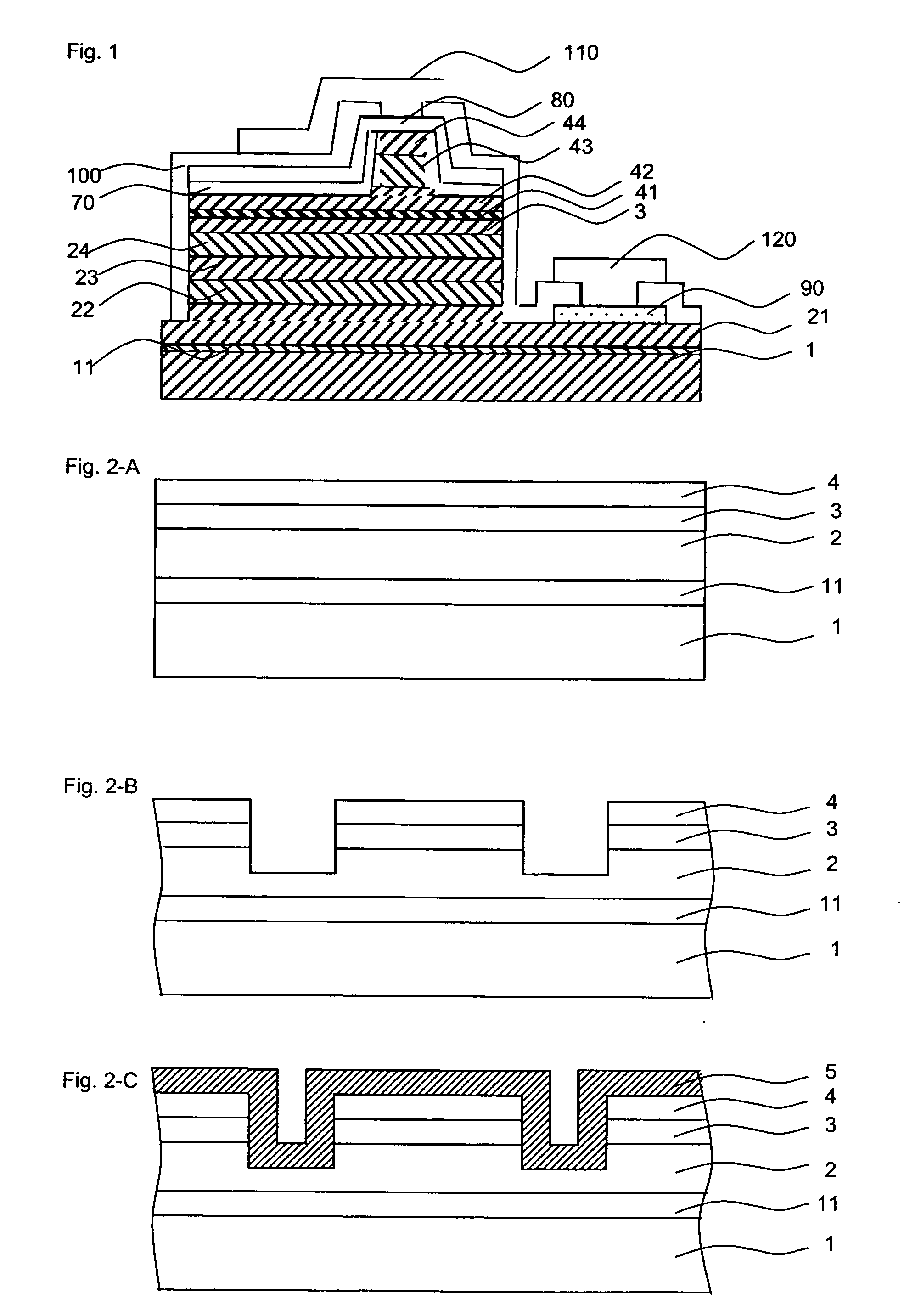
[0109]First, the sapphire wafer 1 of 2 inch diameter and a surface essentially perpendicular to c-axis is placed in the MOCVD reactor. Temperature is set at 510° C. Hydrogen is used as carrier gas and gaseous substrates of the reaction are: ammonia and TMG (thrimethylgallium). The GaN buffer layer 11 of 200 angstrom thick is formed on the sapphire wafer, in the conditions of low-temperature growth.

[0110]On the buffer layer, the following layers are deposited one after the other:[0111](1) 4 μm thick n-type GaN contact layer, doped with Si at the level of 3×10¹⁸ / cm3.[0112](2) 1.5 μm thick undoped In0.06Ga0.94N crack-preventing layer.[0113](3) n-type clad layer, in the form of the superlattice of the total thickness being 1.21 μm, formed by alternate deposition of 25 angstroms thick undoped In0.1Ga0.9N layers and n-type GaN layers doped with Si at the level of 1×10¹⁹ / cm3.[0114](4) 0.2 μm thick undoped n-type GaN optical guide layer of.[0115](5) the active layer of the total thickness b...

example 2

[0131]In this Example 2, only the resonator radiation-emitting end face is covered with a GaN monocrystalline layer, whereas other stages of laser production are carried out as in Example 1. The laser element made in this way is also equipped with a heat sink. Similar as in Example 1, the average lifetime of the laser—with the threshold current density of 2.0 kA / cm2, the power output of 100 mW and the 405 nm light wavelength—is extended.

example 3

[0132]In this Example 3, after the buffer layer is formed on a sapphire wafer, a 100 μm thick GaN layer is deposited by the HVPE method. Next, as in Example 1, the n-type nitride semiconductor layer, the active layer and the p-type nitride semiconductor layer are formed.

[0133]Next, sapphire is removed and consequently a homogenous GaN substrate is obtained. In the successive stages, as in Example 1, resonator end faces are uncovered and subsequently covered with a 0.5 μm thick GaN monocrystalline layer crystallized in the environment of a supercritical ammonia-containing solution. In the case of the nitride semiconductor laser thus obtained, its parameters may be expected to get improved as in Example 1.


PUM


Abstract

The present invention relates to a nitride semiconductor laser device provided with a window layer on a light-emitting end face of the resonator which comprises an active layer of nitride semiconductor between the n-type nitride semiconductor layers and the p-type nitride semiconductor layers, in which at least the radiation-emitting end face of said resonator is covered by said window layer comprising monocrystalline nitride of general formula AlxGa1−x−yINyN, where 0≦x+y≦1, 0≦x≦1 and 0≦y<1, having a wider energy gap than that of the active layer and being formed at a low temperature so as not to damage said active layer. Formation of such a window layer improves significantly the performance of the nitride laser device according to the invention.

Description

BACKGROUND OF THE INVENTION[0001]1. Field of the Invention[0002]The invention relates to a nitride semiconductor laser device and to a method for improving its performance leading to an extension of its lifetime. In particular the method according to the invention relates to providing a window layer on the radiation emitting end face of the resonator. Such a layer increases durability of the nitride semiconductor laser device according to the invention.[0003]2. Description of the Related Art[0004]Lifetime of semiconductor laser devices depends primarily on quality of the optically active layers, and especially on quality of resonator mirrors of such layers. In the so-far used semiconductor laser diodes manufactured on the basis of semiconductors of the GaAs group, extension of the lifetime of a laser diode is achieved by forming special layers on resonator mirrors. These layers are used as antireflection layers or they form a window structure. Such a structure has been disclosed in ...

Claims


Application Information

Patent Timeline
IPC IPC(8): H01S5/00C30B7/00H01L21/208C30B9/00H01S5/028H01S5/16H01S5/323
CPCC30B9/00C30B29/403C30B29/406C30B7/005H01S5/164H01S5/32341H01S5/0281H01S5/30
Inventor DWILINSKI, ROBERTDORADZI SKI, ROMANGARCZY SKI, JERZYSIERZPUTOWSKI, LESZEK P.KANBARA, YASUO
Owner AMMONO SP Z O O (PL)
Why Eureka
Try Eureka