Capacitors With High Energy Storage Density And Low Esr

a technology of energy storage density and capacitors, applied in the field of capacitors with high energy storage density and low esr, can solve the problems of too slow process for making fifty-micron thick films generally associated with such applications, considered far too laborious and slow for commercial purposes, and achieves superior low-defectivity and conformality of ald films, reducing the impact of performance or subsequent packaging process flow, and minimizing adverse effects on device performan

Inactive Publication Date: 2008-04-24
SUNDEW TECH
View PDF7 Cites 38 Cited by
  • Summary
  • Abstract
  • Description
  • Claims
  • Application Information

AI Technical Summary

Benefits of technology

[0020] ALD films can grow continuously at any thickness, provided that the surface of the substrate is made reactive to one of the ALD precursors. In this case, ALD films can be grown with layer-by-layer continuity all the way from the interface. The ability to initiate the surface and start layer-by-layer growth from the first layer makes ALD films continuous, low stress, and pinhole free; thus, it is an ideal candidate for devices with high-capacitance area substrates wherein the reliability and yield crucially depend on the number or density of defects. For example, ALD dielectric films are developed for DRAM capacitor applications wherein they were proven to maintain close to 100% yield for ultrathin films in the range of ˜5 nm over area-enhanced wafers with actual area exceeding 10,000 cm2. Additionally, Al2O3 dielectric films predominantly overtook PVD films in the magnetic data storage industry wherein magnetic sensors are manufactured at practically 100% yield using ALD. Finally, ALD films utilized for device encapsulation applications have shown significant device reliability improvements indicating pin-hole free coatings over large-size flat panel devices, as well as other devices. As a result, very thin encapsulation films can be realized by ALD with minimized adverse impact on device performance. For example, IC devices can be encapsulated at the wafer level with minimized impact on performance or subsequent packaging process flow.
[0021] Given the superior low-defectivity and conformality of ALD films, they are exceptionally suitable for the deposition of dielectric and conductive films for high-energy and capacitance applications.
[0022] It is the objective of the present invention to provide a method for capacitor manufacturing with improved capacitance and energy density while maintaining low ESR. It is another objective of the invention to improve ele...

Problems solved by technology

ALD, up to now, has been considered too slow a process to make the fifty-micron thick films generally associated with such applica...

Method used


Image

  • Capacitors With High Energy Storage Density And Low Esr
  • Capacitors With High Energy Storage Density And Low Esr
  • Capacitors With High Energy Storage Density And Low Esr

Examples


embodiment 450

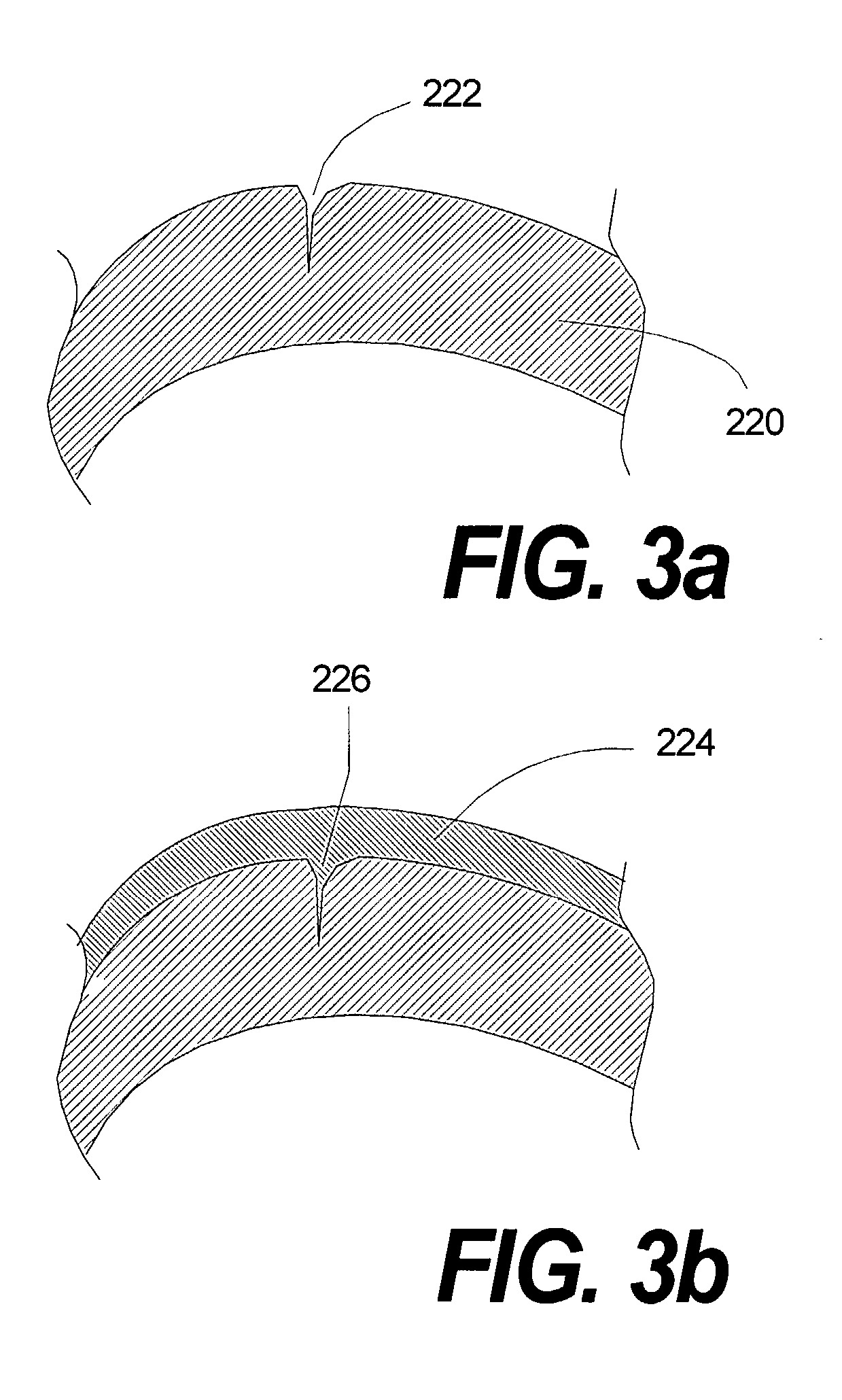
[0062] While the capacitor layout described in reference to FIG. 6a is suitable for low ESR applications, further improvements are obtained by the implementation of thick overlaying films in contact with layer 406. This embodiment further reduces series resistance related to the non-contact fraction of the area 424. The embodiment 450 is illustrated in FIG. 6b. Film 458 is preferably formed over contact layer 406′ without ambient exposure to avoid surface oxidation of layer 406′. For example, layer 458 is formed by sputtering 0.5 μm to 1 μm of aluminum as known to those who are skilled in the art. While this technique achieves substantially higher contact area through fractional area 424′, it is not required to substantially penetrate into the deep high-capacitance area features such as 422′. In some embodiments, film 458 completely replaces foil 408 (FIG. 6a). In most common applications, relatively thin film 458 is implemented with or without a complementary non-oxidizing film at ...

embodiment 1000

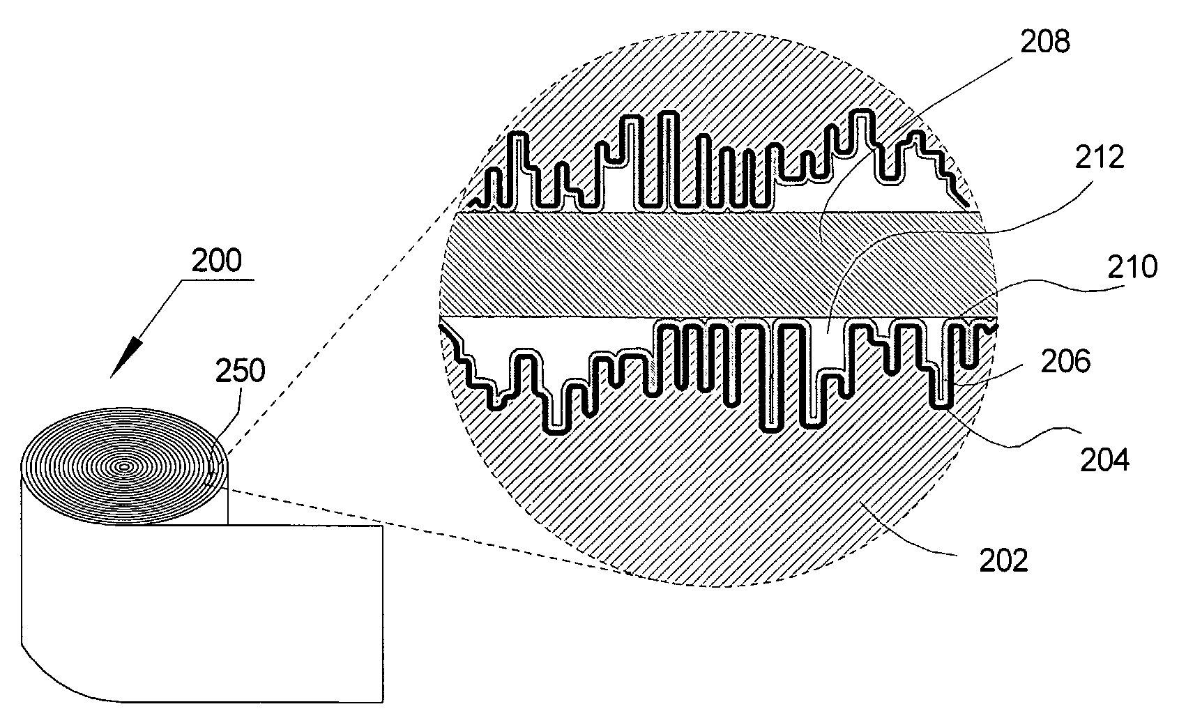
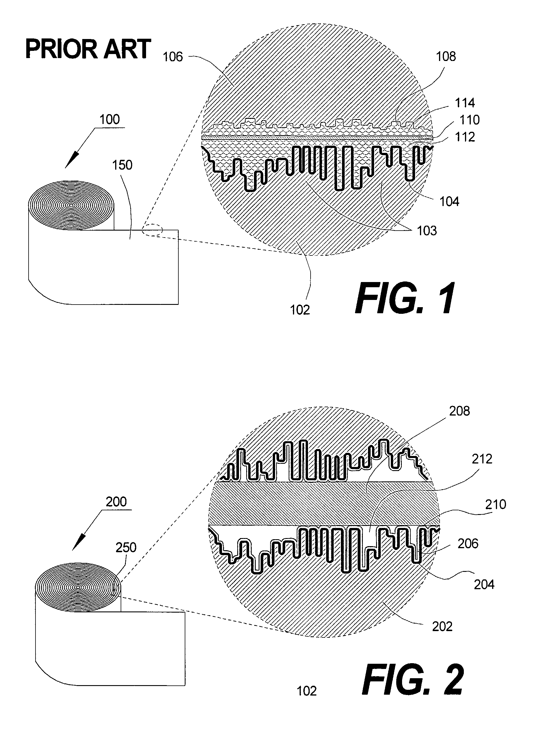
[0077] An objective of this invention is to fabricate high-energy storage capacitors. Advantageously, capacitors that are suitable for high voltage are fabricated over aluminum foils with lower area enhancement foil. For example, 50 μm foils with an etched ×40 area enhancement can accommodate a 1.0 μm thick Al2O3 dielectric layer grown on both sides of the foil by ALD or combination of anodic-oxidation and ALD as described above. Derated at 50%, these dielectric films are suitable for the fabrication of 500V capacitors. Low ESR contact is established, for example, by implementing a 50 nm TiN contact layer deposited by ALD followed by 0.5 μm of copper deposited by a combination of 10 nm seed ALD layer and electroplating and by utilizing a commercially available 5.8 μm thick aluminum foil 208 (FIG. 2). Accordingly, capacitance per area is 0.56 μF / cm2. The thickness of the stack is ˜56 μm and the weight per area is 0.01 gram / cm2. A capacitor with 400 μF is formed by winding 1 cm wide s...


PUM

PropertyMeasurementUnit
Lengthaaaaaaaaaa
Thicknessaaaaaaaaaa
Dielectric polarization enthalpyaaaaaaaaaa

Abstract

Electrostatic capacitors with high capacitance density and high-energy storage are implemented over conventional electrolytic capacitor anode substrates using highly conformal contact layers deposited by atomic layer deposition. Capacitor films that are suitable for energy storage, electrical and electronics circuits, and for integration onto PC boards endure long lifetime and high-temperature operation range.

Description

BACKGROUND OF THE INVENTION [0001] 1. Field of the Invention [0002] This invention relates to the area of electronic components and more specifically to apparatus and method for constructing capacitors with high capacitance and high-energy storage density as well as low equivalent series resistance. [0003] 2. Description of Prior Art [0004] Capacitor devices have a host of applications in the electrical, electronics, and microelectronics arts. Many different useful implementations of capacitors were successfully implemented and commercialized. Capacitor properties such as capacitance density, operating voltage, energy storage density, equivalent series resistance (ESR), temperature resilience, and lifetime were constantly improved. Concurrently, substantial drive to reduce the cost and the size of capacitors drove the technology into substantially automatic manufacturing methods and achieved satisfactory commodity status for most applications. [0005] Capacitors are useful for energy...

Claims


Application Information

Patent Timeline
IPC IPC(8): H01G4/008H01G4/00H01G9/055
CPCH01G4/10H01G4/30Y10T29/43H01G9/055Y10T29/435H01G4/32H01G9/045
Inventor SNEH, ANATSNEH, OFER
Owner SUNDEW TECH
Why Eureka
Try Eureka