Correlated electron memory

a technology of electron memory and correlation, applied in the field of integrated circuit memory, can solve the problem that the skill of memory art is generally unfamiliar to the general publi

Active Publication Date: 2008-05-08
SYMETRIX MEMORY
View PDF9 Cites 276 Cited by
  • Summary
  • Abstract
  • Description
  • Claims
  • Application Information

AI Technical Summary

Problems solved by technology

Because these materials have never before been used in a memory, t

Method used


Image

  • Correlated electron memory
  • Correlated electron memory
  • Correlated electron memory

Examples


example i

[0075]A 2000 Å (Angstrom) layer of platinum was deposited on a wafer with a silicon dioxide coating. Then a 0.2 molar nickel oxide precursor in an octane solution was deposited by spin coating the platinum layer at 3000 rpm (rounds per minute). The nickel oxide precursor is available from Kojundo Chemical Company, Tokyo, Japan. The precursor was baked at 150° C. for 1 minute, and then at 260° C. for four minutes to produce an approximately 100 Å dry layer. The spin-on deposition and baking processes were repeated six times for a total thickness of 600 Å. Then a crystallization anneal was performed in a furnace at 450° C. in an oxygen atmosphere for 40 minutes to produce a 600 Å layer of the CEM nickel oxide according to the invention. Electron microscopy revealed that a significant amount of carbon was present in the material, with the carbon coming from the octane precursor. A top electrode of 2000 Å of platinum was deposited. Then the top electrode and CEM layer were patterned by ...

example ii

[0076]This example was made in the same way as Example I above except that 5% ammonia was added to the precursor. The films produced yielded similar results.

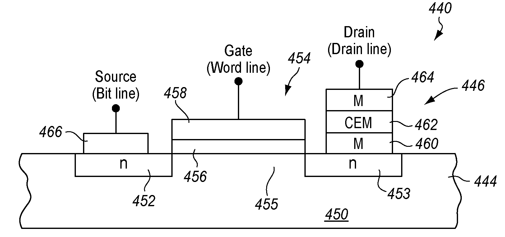
[0077]The invention includes an annealing process for CEMs. The CEM may be annealed in a gas containing at least one chemical element for forming a ligand which stabilizes the electronic properties of the CEM. Preferably, the CEM is a transition metal and the chemical element comprises carbon. Preferably, the gas comprises a gas selected from CO and CO2. Preferably, the CEM is nickel.

[0078]The invention also provides a sputtering method of making a CEM. The material may be sputtered and then annealed as described above, or reactive sputtering of the CEM in a gas containing at least one chemical element for forming a ligand which stabilizes the electronic properties of the CEM may be employed. Preferably, the CEM is a transition metal and the chemical element comprises carbon. Preferably, the gas comprises a gas selected from CO ...


PUM


Abstract

A non-volatile resistive switching memory that includes a homogeneous material which changes between the insulative and conductive states due to correlations between electrons, particularly via a Mott transition. The material is crystallized into the conductive state and does not require electroforming.

Description

CROSS-REFERENCE TO RELATED APPLICATIONS[0001]This Application is a Non-Provisional Application claiming the benefit of: Provisional (35 USC 119(e)) Application No. 60 / 858218 filed on Nov. 8, 2006; Provisional (35 USC 119(e)) Application No. 60 / 904768 filed on Mar. 2, 2007; Provisional (35 USC 119(e)) Application No. 60 / 906158 filed on Mar. 9, 2007; and Provisional (35 USC 119(e)) Application No. 60 / 913245 filed on May 21, 2007. All of the foregoing provisional applications are hereby incorporated by reference to the same extent as though fully disclosed herein.FIELD OF THE INVENTION[0002]The invention in general relates to integrated circuit memories, and in particular, to the formation of non-volatile integrated circuit memories containing materials which exhibit a change in resistance.BACKGROUND OF THE INVENTION[0003]Non-volatile memories are a class of integrated circuits in which the memory cell or element does not lose its state after the power supplied to the device is turned ...

Claims


Application Information

Patent Timeline
IPC IPC(8): G11C11/00H01L21/00
CPCH01L45/04H01L45/1233H01L45/146H01L45/1608H01L27/2436H01L45/1625H01L45/1641H01L45/1675H01L27/2409H01L45/1616H10B63/20H10B63/30H10N70/20H10N70/021H10N70/026H10N70/023H10N70/041H10N70/826H10N70/8833
Inventor PAZ DE ARAUJO, CARLOS A.CELINSKA, JOLANTABRUBAKER, MATTHEW D.
Owner SYMETRIX MEMORY
Why Eureka
Try Eureka