

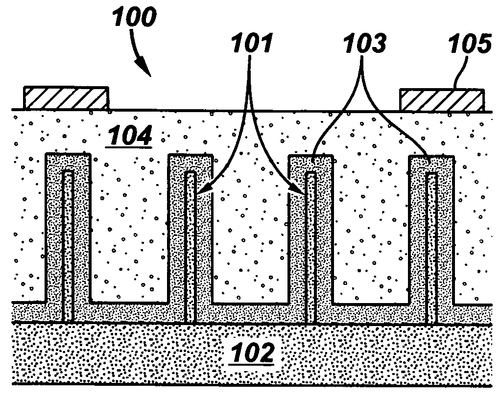
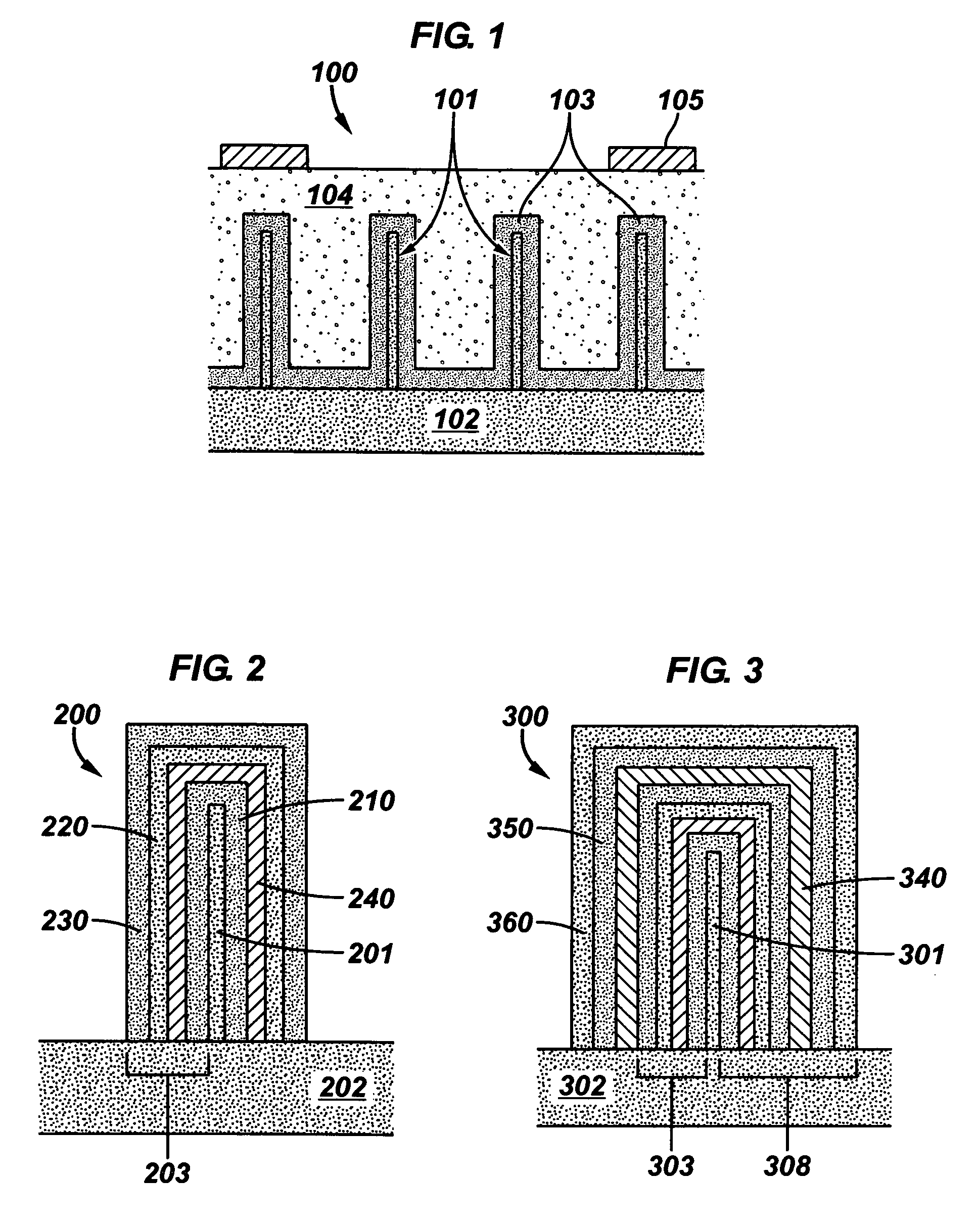
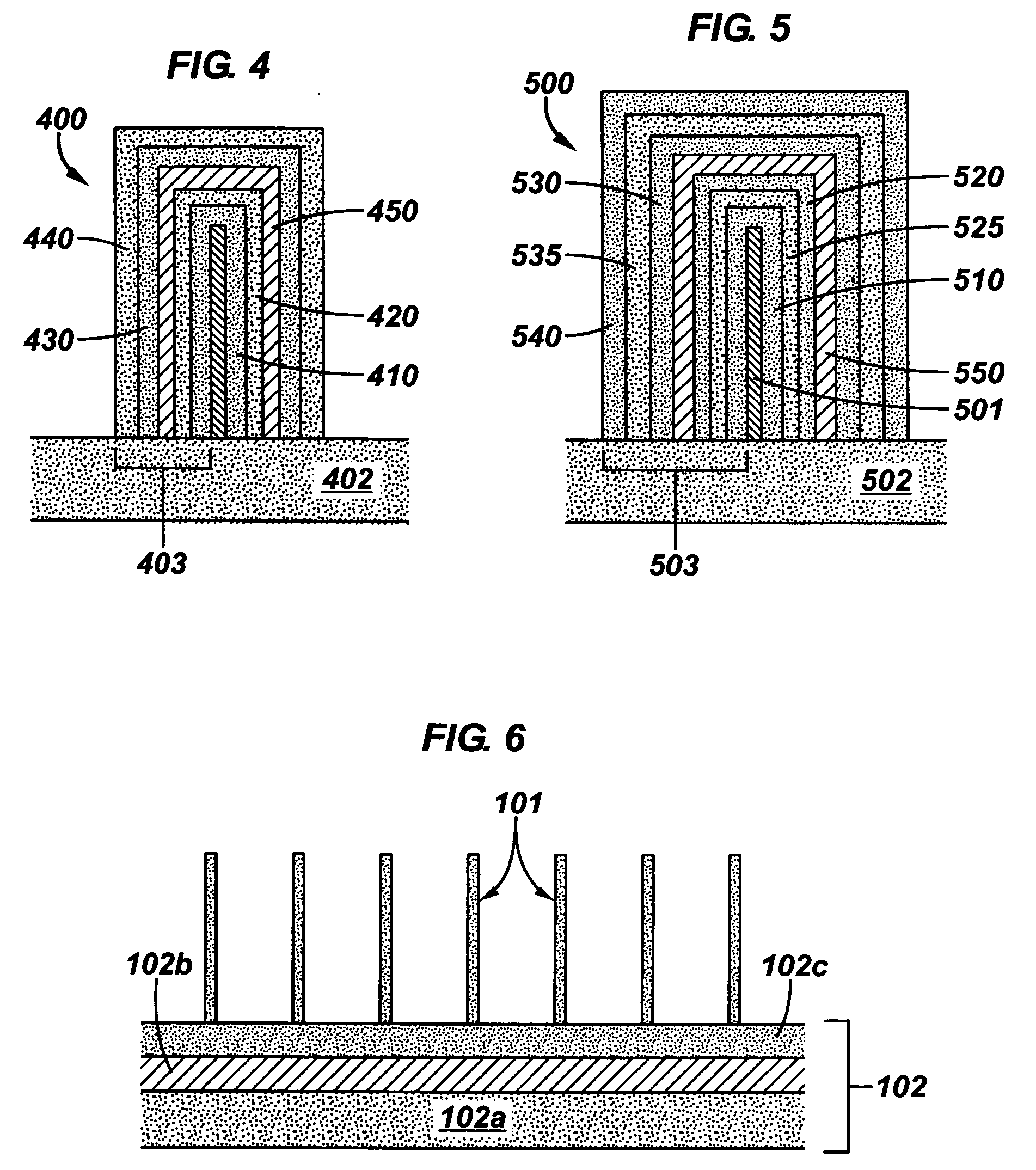
Amorphous-crystalline tandem nanostructured solar cells
a tandem nanostructured, crystalline technology, applied in the field of solar cells, can solve the problems of charge carrier recombination, insufficient efficiency to significantly reduce the cost involved in the production and the competition from conventional sources of electricity preclude the widespread use of such solar cell technology, etc., to achieve the effect of optimizing light absorption and broad spectrum
- Summary
- Abstract
- Description
- Claims
- Application Information
AI Technical Summary
Benefits of technology
Problems solved by technology
Method used
Image

Examples
example 1
[0075]The following experimental example is included to demonstrate embodiments for the growth of nanowires as disclosed herein. They are intended to be exemplary of the present invention, and thus not limiting. FIG. 8a shows the growth of long, high density silicon nanowires having an average diameter of 57 nm. FIG. 8b, shows shorter, low density silicon nanowires having an average diameter of 182 nm. Finally, FIG. 8c demonstrates a randomized array of silicon nanowires with an average diameter of 70 nm.
example 2
[0076]The following experimental example is included to demonstrate embodiments for the conformal deposition of layers about nanowires as disclosed herein. They are intended to be exemplary of the present invention, and thus not limiting. FIG. 9a shows high density wires with conformally deposited a-Si on long high density silicon nanowires. FIG. 9b shows a cross-sectional view of conformally deposited a-Si on a c-Si nanowire 900. The a-Si layer was introduced by CVD. The first layer of a-Si 910 is an intrinsic and the second layer 920 is n-doped.
PUM
| Property | Measurement | Unit |
|---|---|---|
| width | aaaaa | aaaaa |
| width | aaaaa | aaaaa |
| angle | aaaaa | aaaaa |
Abstract
Description
Claims
Application Information