Local coloring for hierarchical opc

Inactive Publication Date: 2008-06-05
GLOBALFOUNDRIES INC
View PDF21 Cites 17 Cited by
  • Summary
  • Abstract
  • Description
  • Claims
  • Application Information

AI Technical Summary

Benefits of technology

[0027]Bearing in mind the problems and deficiencies of the prior art, it is therefore an object of the present invention to provide a me

Problems solved by technology

The resolution of an exposure system is limited by the contrast of the projected light image, that is, the intensity difference between adjacent light and dark features.
Thus such algorithms have been difficult to effectively automate.
Currently phase coloring is considered a binary design problem and uses nets and net coloring to form the mask.
Of course, such a data structure for a VLSI device is extremely complex, and could contain millions of shapes for each mask, with several masks required for each device.
These systems simplify the complex task of designing VLSI devices, but have traditionally had problems analyzing the hierarchical design.
However, as design density increases, subnet sizes increase and the probability of finding a clean coloring solution is significantly diminished, and flattening bec

Method used


Image

  • Local coloring for hierarchical opc
  • Local coloring for hierarchical opc
  • Local coloring for hierarchical opc

Examples


Embodiment Construction

)

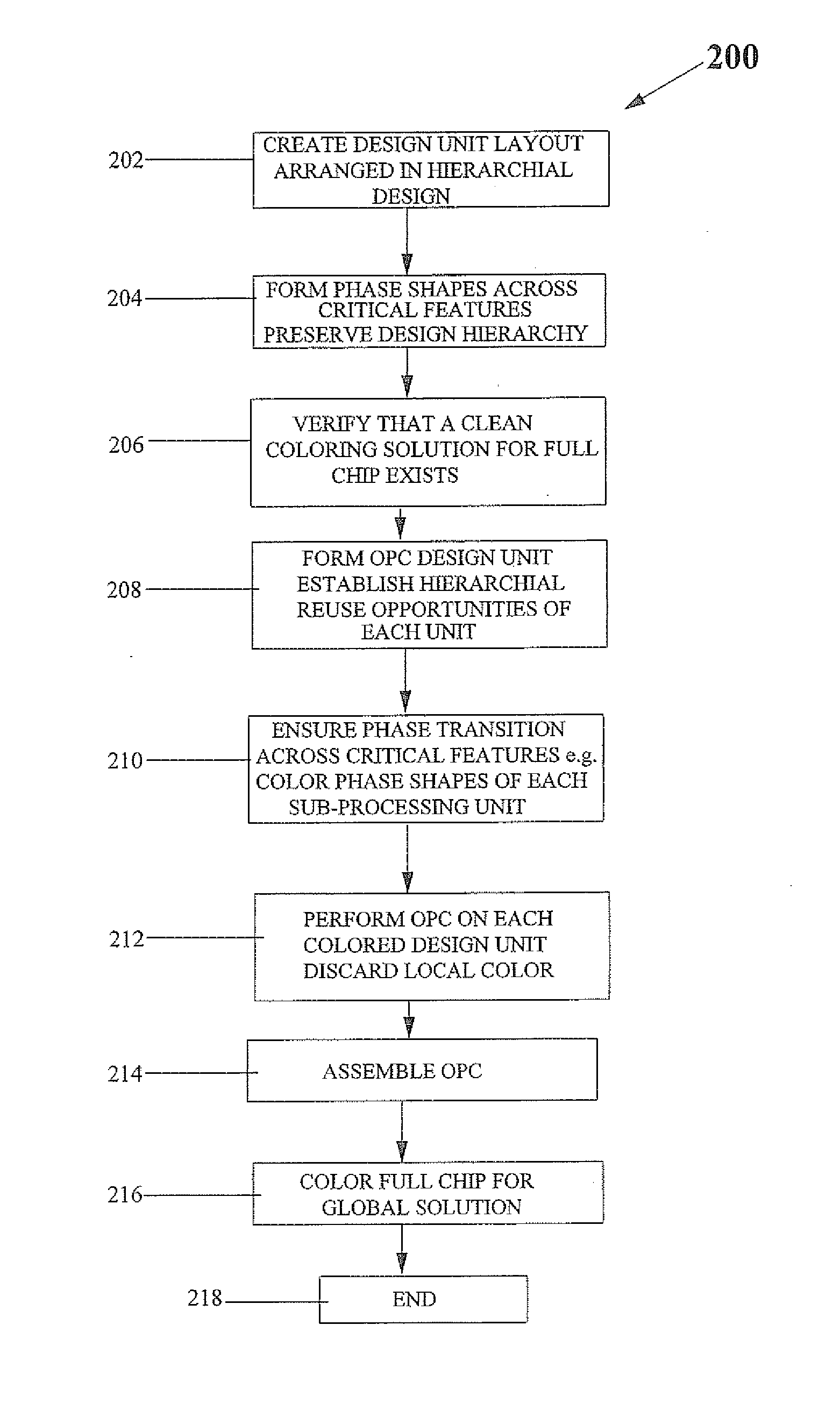
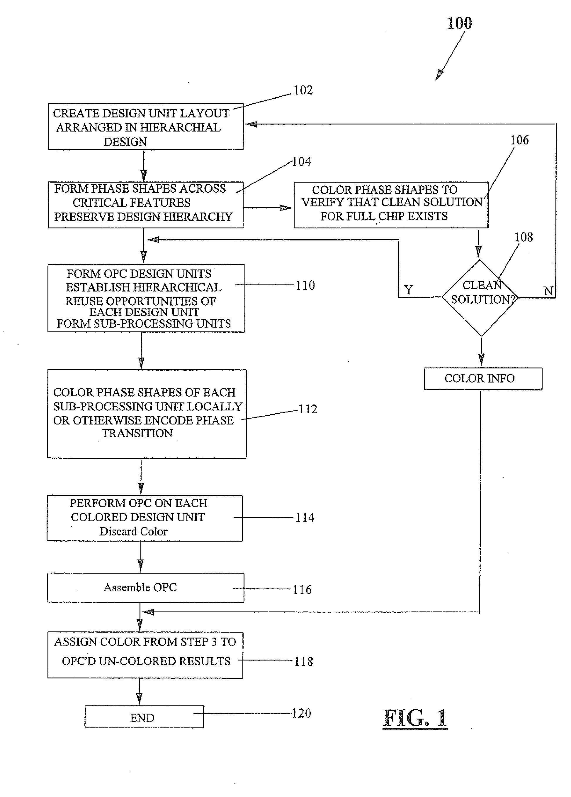
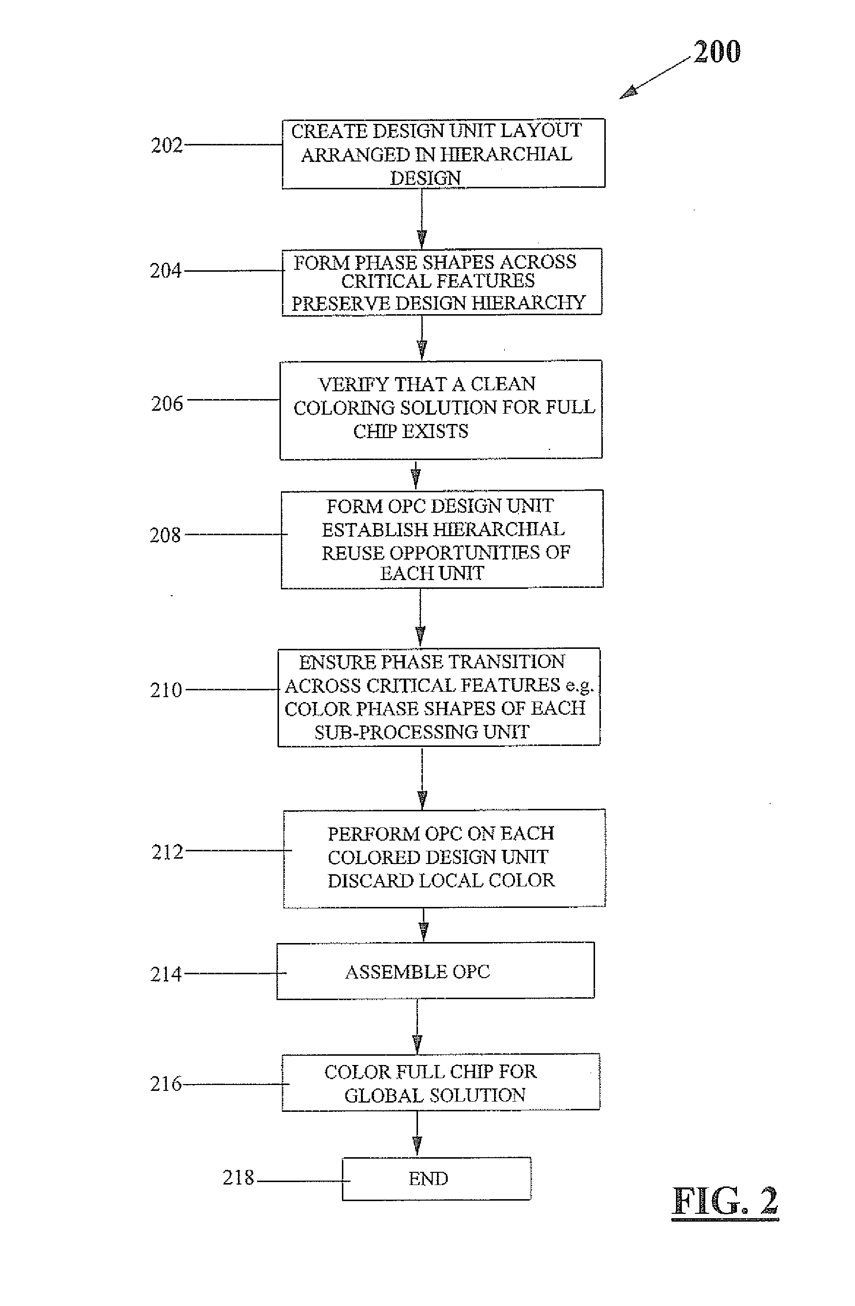
[0049]The present invention and the various features and advantageous details thereof are explained more fully with reference to the nonlimiting embodiments that are illustrated in the accompanying drawings and detailed in the following description. It should be noted that the features illustrated in the drawings are not necessarily drawn to scale. Descriptions of well-known components and processing techniques are omitted so as to not unnecessarily obscure the present invention. The examples used herein are intended merely to facilitate an understanding of ways in which the invention may be practiced and to further enable those of skill in the art to practice the invention. Accordingly, the examples should not be construed as limiting the scope of the invention. In particular, embodiments are described with respect to alternating phase shift mask (altPSM) design, but the invention is applicable to the design of other masks that require coloring, including, but not limited to, deco...


PUM


Abstract

A method for designing a mask for fabricating an integrated circuit is provided wherein a mask layout that requires coloring, such as for alternating phase shift, double-exposure and double-exposure-etch masks, is organized into uncolored hierarchical design units. Prior to modification by OPC, each hierarchical design unit is locally colored. OPC is then performed on the locally colored hierarchical design unit. The local coloring information for the hierarchically arranged OPC-modified design unit may be discarded. After OPC modification, the uncolored OPC-modified design units may be placed within the mask layout, and the flattened data may be colored. Thus, turnaround time for mask design is significantly improved since the numerically intensive OPC is performed on the hierarchical data, avoiding the need to perform OPC on flattened data, whereas the less intensive global coloring is performed on flattened data.

Description

BACKGROUND OF THE INVENTION [0001]1. Field of the Invention[0002]This invention generally relates to VLSI circuit design and more specifically relates to optical proximity correction in the design of lithographic masks that require coloring, for example, in alternating phase shift masks or double exposure masks.[0003]2. Description of Related Art[0004]Integrated circuits including very large scale integrated (VLSI) complementary metal oxide semiconductor (CMOS) devices are manufactured on a silicon wafer by a sequence of material additions (i.e., low pressure chemical vapor depositions, sputtering operations, etc.), material removals (i.e., wet etches, reactive ion etches, etc.), and material modifications (i.e., oxidations, ion implants, etc.). These physical and chemical operations interact with the entire wafer. For example, if a wafer is placed into an acid bath, the entire surface of the wafer will be etched away. In order to build very small electrically active devices on the ...

Claims


Application Information

Patent Timeline
IPC IPC(8): G06F17/50
CPCG03F1/36G03F1/144
Inventor BAUM, ZACHARYGRAUR, IOANALIEBMANN, LARS W.MANSFIELD, SCOTT M.
Owner GLOBALFOUNDRIES INC
Why Eureka
Try Eureka