Glass-sealed light emitting element, circuit board with the glass-sealed light emitting element, and methods for manufacturing those

a technology of light emitting element and glass shell, which is applied in the manufacture of electrode systems, electric discharge tubes/lamps, and discharge tubes luminescnet screens. it can solve the problems of silicone resins, silicone resins, and conventionally used sealing resins, and achieve excellent light resistance, reduce luminance, and improve the effect of light taking efficiency

Inactive Publication Date: 2008-06-12
ASAHI GLASS CO LTD
View PDF10 Cites 17 Cited by
  • Summary
  • Abstract
  • Description
  • Claims
  • Application Information

AI Technical Summary

Benefits of technology

[0038]In accordance with the present invention, it is possible to use, as the sealing material for a light emitting diode, a glass material, which is excellent in light resistance.
[0039]Thus, it is possible to control the directivity of emission light with a light emitting element being used as a light source. By adopting a glass material, it is possible to solve the problem of, e.g., a decrease in luminance due to the discoloration of the conventional sealing resins. If glass having a high refractive index is used, it is possible to improve the efficiency of taking light out of a light emitting element.
[0040]Further, since glass materials have a better thermal conductivity than resins, it is possible to improve the heat dissipation that has been a problem of, in particular, high luminance LEDs. When color conversion materials are dispersed in glass, it is possible not only to mix an emission color and a converted color to obtain a desired color but also to improve the heat dissipation as an electronic device. As stated above, it is possible to fabricate a light emitting element sealed by glass, which is excellent in at least one of light resistance, light out-coupling efficiency and heat dissipation. Further, it is possible to control the directivity of emission light by forming a light emitting element in a certain curved shape.

Problems solved by technology

However, there has been a problem in terms of the degradation of a sealing resin used in a light emitting diode.
Epoxy resins, which have been conventionally used, are more likely to be decomposed by blue light or ultraviolet light.
However, even the silicone resins are subjected to a decrease in the amount of emission light caused by discoloration.
In particular, the decrease has caused a serious problem in light emitting diodes having a short wavelength and a high luminance.
For this reason, the light out-coupling efficiency is low.
Furthermore, the conventional sealing resins have a low thermal conductivity, resulting in a poor heat resistance and discoloration due to a temperature increase, and consequently luminance degradation.
In this case, since emission light from a light emitting diode directly goes into a medium having a low refractive index of 1, such as air or nitrogen, once, the component reflected by an interface occupies a large part of the emission light, significantly reducing the light out-coupling efficiency.
In addition, there remains the problem of heat resistance.
However, since the light emitting element 1010 and the bonding wires 1023, 1024 are all covered with low melting glass in Patent Document 3, there is a possibility that a bonding wire breaks.
From this point of view, it is supposed that it is difficult to sufficiently increase the directivity of emission light from the light emitting element 1010.

Method used


Image

  • Glass-sealed light emitting element, circuit board with the glass-sealed light emitting element, and methods for manufacturing those
  • Glass-sealed light emitting element, circuit board with the glass-sealed light emitting element, and methods for manufacturing those
  • Glass-sealed light emitting element, circuit board with the glass-sealed light emitting element, and methods for manufacturing those

Examples


example 1

[0095]FIG. 8 is a flowchart showing an example of the fabrication process of the glass-sealed light emitting diode chip and the circuit board with the light emitting diode according to the present invention. FIG. 9 is a graph showing the history of a substrate temperature in the fabrication process.

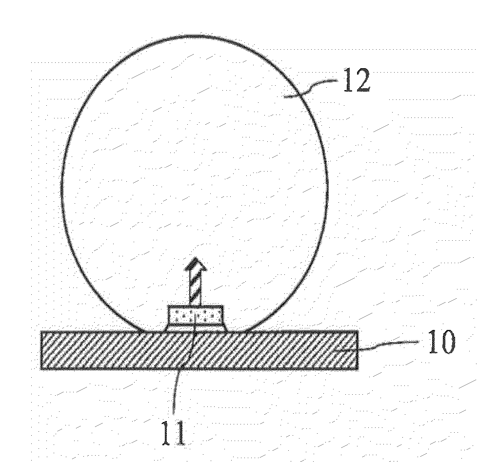
[0096]First, a substrate with a releasing agent applied thereon was fabricated (Step S1). The substrate comprised a 6-inch silicon wafer manufactured by OSAKA TITANIUM, and boron nitride powder “Boron Spray” manufactured by KakenTech Co. Ltd. was sprayed as the releasing agent on the silicon wafer. The boron nitride powder was sprayed such that the silicon wafer surface was not seen. Next, a glass member for sealing was fabricated. The glass material for the glass member had a composition of TeO2 (45.0%), TiO2 (1.0%), GeO2 (5.0%), B2O3 (18.0%), Ga2O3 (6.0%), Bi2O3 (3.0%), ZnO (15%), Y2O3 (0.5%), La2O3 (0.5%), Gd2O3 (3.0%) and Ta2O5 (3.0%).

[0097]The rate “%” means “mol %”. The glass member...

example 2

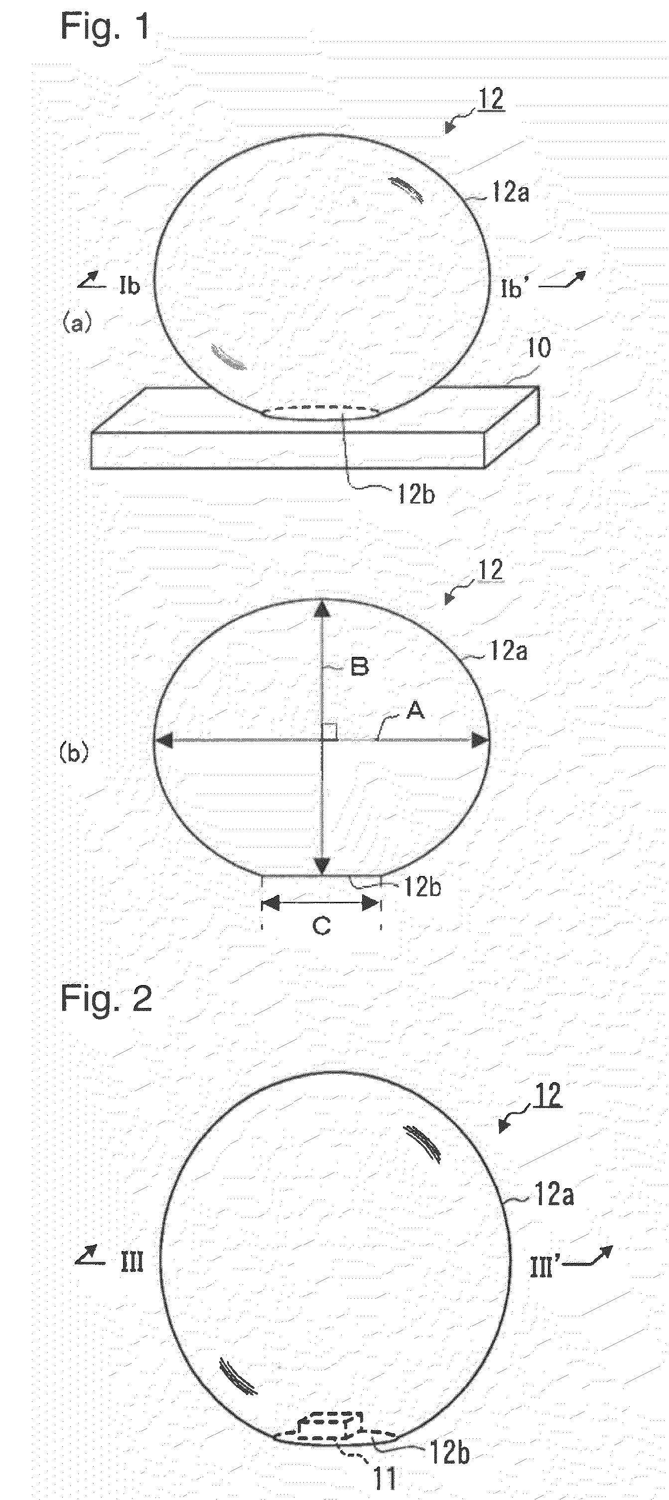
[0109]After cullet comprising the same material as the glass material used in Example 1 was crushed in a mortar by a pestle, a yellow phosphor material “P46-Y3” manufactured by Kasei Optonix, Ltd. having a weight of 381 mg was mixed into the crushed cullet to obtain a phosphor-containing frit. The obtained phosphor-containing glass frit was divided into parts having a weight of 34 mg, the divided parts were heated at 610° C. for 15 minutes. The temperature-raising rate and the cooling rate were set at the same rates as those in Example 1. Thus, glass members were formed in a shape as shown in FIG. 1(a).

[0110]When light emitting diode chips and the above-mentioned glass members were put on a substrate coated with a releasing agent as in Example 1, light emitting diode chips were obtained, being sealed by glass members with phosphor dispersed therein. The turn-on voltage was 2.4 V, and white light emission was obtained.

[0111]Blue rays, which were emitted from a light emitting diode ch...

example 3

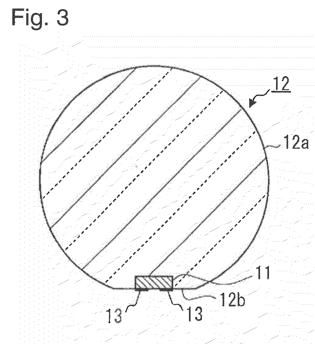
[0113]Boron nitride powder was sprayed, as a releasing agent, on an inner wall of a cylindrical pipe 53, which had an inner diameter 5.5 mm, a thickness of 0.5 mm and a height of 10 mm, and which was available under the tradename of Pyrex (FIG. 14(a)), and the pipe was put on a substrate 50, which had a light emitting diode chip carried thereon and was coated with a releasing agent. After that, a glass material containing the same composition as that of Example 1 and having a weight of 381 mg, was filled in the pipe 53, was heated and was cooled along with the chip. The pipe 53 and the substrate 50 formed a jig 54 for forming a glass member. The heating condition and the cooling condition were the same those of Example 1.

[0114]After cooling, a light emitting diode chip was obtained, being sealed with glass, which had a leading portion formed in a curved shape by surface tension as shown in FIG. 14(b). Reference numeral 51 designates the light emitting diode chip, and reference numer...


PUM

PropertyMeasurementUnit
refractive indexaaaaaaaaaa
softening pointaaaaaaaaaa
refractive indexaaaaaaaaaa

Abstract

A diode chip is sealed by a glass material.
There are provided a light emitting diode chip and a glass member in close contact with at least one portion of the surface of the light emitting diode chip. The glass member has a surface shape containing a curved surface at least a portion thereof. The curved surface is preferably a portion of a spherical surface or a spheroidal surface. The glass member has a surface shape containing a spherical portion and a flat portion, and the diode chip is preferably disposed on the flat portion.

Description

BACKGROUND OF THE INVENTION[0001]1. Field of the Invention[0002]The present invention relates to a glass-sealed light emitting element, a circuit board with the glass-sealed light emitting element, a method for manufacturing the glass-sealed light emitting element, and a method for mounting the glass-sealed light emitting element.[0003]2. Discussion of Background[0004]A light source using a light emitting diode (hereinbelow, referred to as LED lamp) is a small and highly efficient light source. The LED lamp is highly reliable since there is no danger of blowout for example. Blue light emitting diodes have been recently developed. A light source for a full-color display can be fabricated by combining blue light emitting diodes and conventional green and red light emitting diodes.[0005]On the other hand, there has been disclosed a method for obtaining white light emission by combining blue light emission and a color conversion material (see Patent Document 1 identified below). White L...

Claims


Application Information

Patent Timeline
Patent Type & Authority Applications(United States)
IPC IPC(8): H01L33/00H01L33/54H01L33/56H01L33/58
CPCC03C3/253C03C27/00H01L33/58H01L33/56H01L33/54H01L2224/0554H01L2224/05568H01L2224/05573H01L2224/16225H01L2224/32257H01L2224/48091H01L2224/48247H01L2224/48257H01L2924/00014H01L2924/181H01L2224/05599H01L2924/00012H01L2224/0555H01L2224/0556
Inventor NAKAMURA, NOBUHIROMATSUMOTO, SYUJIONODA, HITOSHISEGAWA, YUTAKAMATSUMOTO, TETSUROUSUI, HIROSHI
Owner ASAHI GLASS CO LTD
Why Eureka
Try Eureka