
Directional crystallization of silicon sheets using rapid thermal processing

a technology of crystallization and silicon sheet, applied in the direction of crystal growth process, final product manufacturing, gel state, etc., can solve the problems of limiting the use of solar cells, reducing the cost of silicon wafer based photovoltaic modules, and the amount of current produced, so as to facilitate the production of a small number of nuclei, improve material properties such as grain size and orientation, and improve the effect of material properties

Inactive Publication Date: 2008-06-19
APPLIED MATERIALS INC
View PDF23 Cites 19 Cited by
  • Summary
  • Abstract
  • Description
  • Claims
  • Application Information

AI Technical Summary

Benefits of technology

[0010]The present invention provides a method of recrystallizing a silicon film or sheet, and in particular crystallizing a small grained crystalline and / or amorphous silicon sheet to improve material properties such as grain size and orientation. According to one aspect, the method includes using rapid thermal processing (RTP) to melt and recrystallize one or more entire silicon sheet(s) in one heating sequence. According to another aspect, the method includes controlling a temperature drop across the thickness of the sheet so as to facilitate the production of a small number of nuclei in the molten silicon and their growth into large grains in a direction normal to the horizontal surface of the film or sheet. According to a further aspect, the invention includes a re-crystallization chamber in an overall process flow that enables high-throughput processing of silicon sheets having desired properties for applications such as photovoltaic modules.

Problems solved by technology

However, other types of modules such as thin-film based solar cells are being explored because of their promise of lower cost, albeit while providing lower efficiencies than silicon based modules.
Therefore, reducing the cost of silicon wafer based photovoltaic modules, particularly their manufacturing costs, is a major challenge in keeping such modules commercially viable.
For high speed ribbon type silicon substrate forming processes to be viable, the challenge is to reach sufficient substrate quality and solar cell efficiency to provide low cost solar electricity.
Similarly, silicon sheets obtained using other ribbon technologies have many small grains, which potentially limit their use in solar cell applications.
As shown in FIG. 1A, when sheet 20 is further processed to form a solar cell and used to provide power to a load RL coupled thereto or to a photovoltaic module comprising sheet 20, the small grains 24, particularly those having grain boundaries normal to the direction of charge carrier flow, will decrease the amount of current produced, and thus limit the efficiency of the module.
However, this process is slow and also introduces stress in the film, among other problems.
Moreover, such recrystallization processes cannot reliably improve grain structure with respect to certain desired properties, such as the reduction of grain boundaries normal to the direction of charge carrier flow in a solar cell.
However, SPC processing is also slow and not as effective in reducing film defects such as dislocations.

Method used


Image

  • Directional crystallization of silicon sheets using rapid thermal processing
  • Directional crystallization of silicon sheets using rapid thermal processing
  • Directional crystallization of silicon sheets using rapid thermal processing

Examples


Embodiment Construction

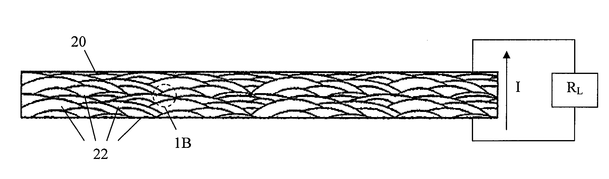
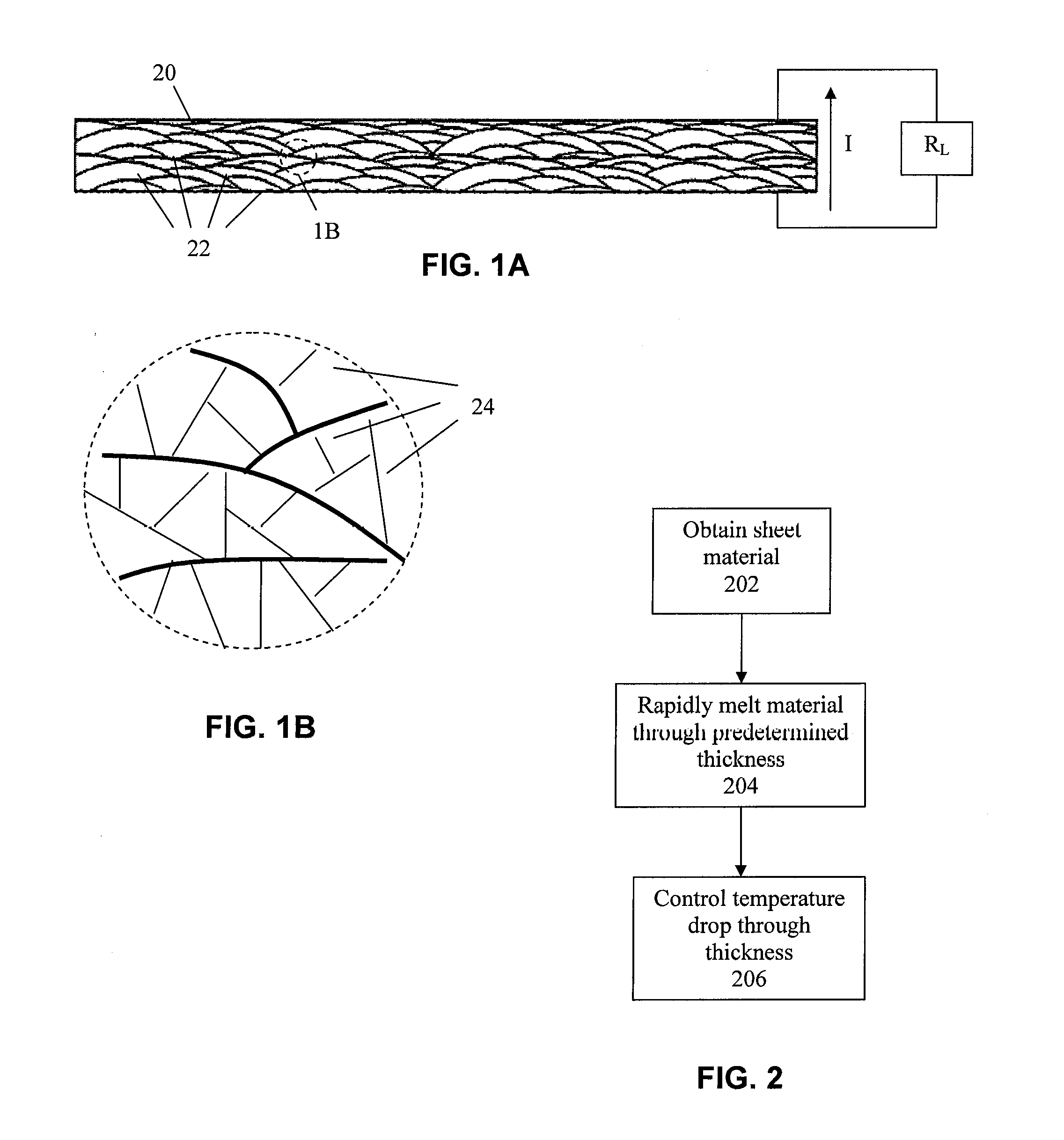
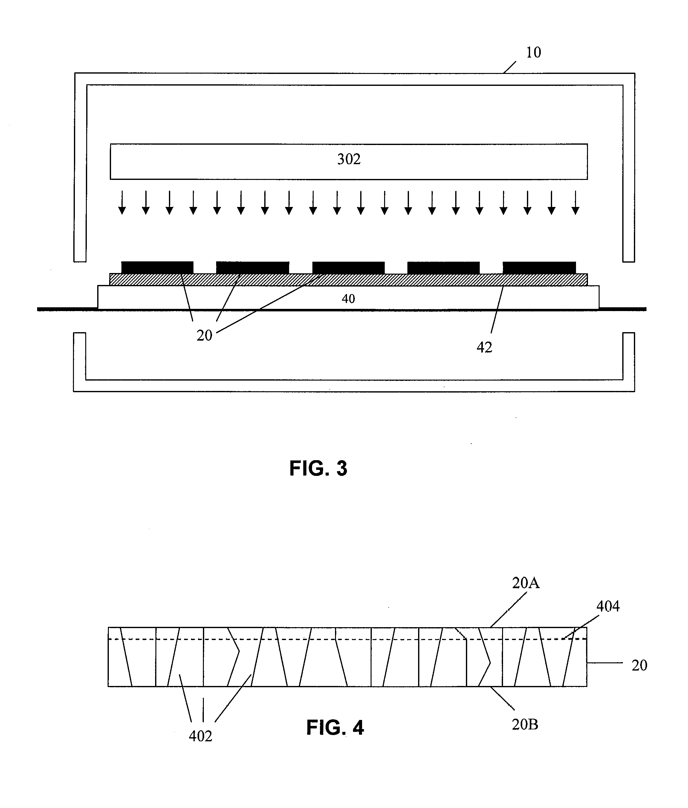
[0017]The present invention will now be described in detail with reference to the drawings, which are provided as illustrative examples of the invention so as to enable those skilled in the art to practice the invention. Notably, the figures and examples below are not\ meant to limit the scope of the present invention to a single embodiment, but other embodiments are possible by way of interchange of some or all of the described or illustrated elements. Moreover, where certain elements of the present invention can be partially or fully implemented using known components, only those portions of such known components that are necessary for an understanding of the present invention will be described, and detailed descriptions of other portions of such known components will be omitted so as not to obscure the invention. In the present specification, an embodiment showing a singular component should not be considered limiting; rather, the invention is intended to encompass other embodime...


PUM

PropertyMeasurementUnit
Grain sizeaaaaaaaaaa
Temperatureaaaaaaaaaa
Thicknessaaaaaaaaaa

Abstract

The present invention provides a method of recrystallizing a silicon sheet, and in particular recrystallizing a small grained silicon sheet to improve material properties such as grain size and orientation. According to one aspect, the method includes using rapid thermal processing (RTP) to melt and recrystallize one or more entire silicon sheet(s) in one heating sequence. According to another aspect, the method includes directionally controlling a temperature drop across the thickness of the sheet so as to facilitate the production of a small number of nuclei in the melted material and their growth into large grains. According to a further aspect, the invention includes a re-crystallization chamber in an overall process flow that enables high-throughput processing of silicon sheets having desired properties for applications such as photovoltaic modules.

Description

FIELD OF THE INVENTION[0001]The present invention relates generally to photovoltaic devices, and more particularly to a method for crystallizing silicon in a silicon sheet by directional solidification using rapid thermal processing (RTP).BACKGROUND OF THE INVENTION[0002]Photovoltaics (PV) or solar cells are devices which convert sunlight into direct current (DC) electrical power. A typical PV cell includes a p type silicon wafer, substrate or sheet typically less than about 0.3 mm thick with a thin layer of n-type silicon on top of a p-type region formed in a substrate. The generated voltage, or photo-voltage, and generated current by the photovoltaic device are dependent on the material properties of the p-n junction and the surface area of the device. When exposed to sunlight (consisting of energy from photons), pairs of free electrons and holes are generated in the silicon. The electric field formed across the depletion region of p-n junction separates the free electrons and hol...

Claims


Application Information

Patent Timeline
IPC IPC(8): B01D9/00H01L25/00
CPCY02E10/547H01L31/1804Y02P70/50
Inventor RANA, VIRENDRA V.BACHRACH, ROBERT Z.
Owner APPLIED MATERIALS INC
Features
  • Generate Ideas
  • Intellectual Property
  • Life Sciences
  • Materials
  • Tech Scout
  • Unparalleled Data Quality
  • Higher Quality Content
  • 60% Fewer Hallucinations
Learn More