

Embedded semiconductor memory devices and methods for fabricating the same
a technology of semiconductor memory and embedded semiconductor, which is applied in the field of semiconductor memory devices, can solve the problems of low memory storage density, complicated array arrangement, and large size of logic compatible flash memory cells, and achieve the effect of high density data storag
- Summary
- Abstract
- Description
- Claims
- Application Information
AI Technical Summary
Benefits of technology
Problems solved by technology
Method used
Image

Examples
second embodiment
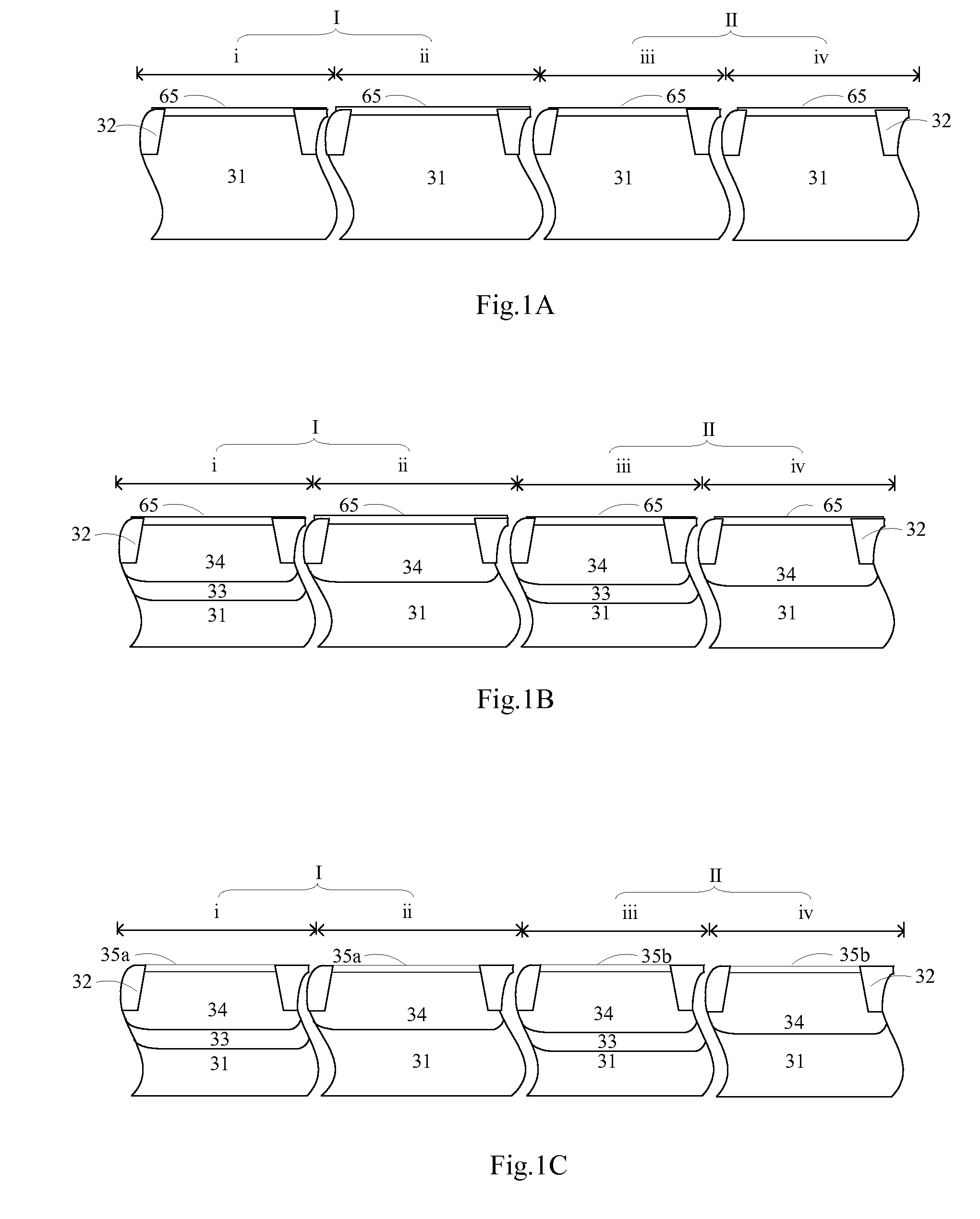
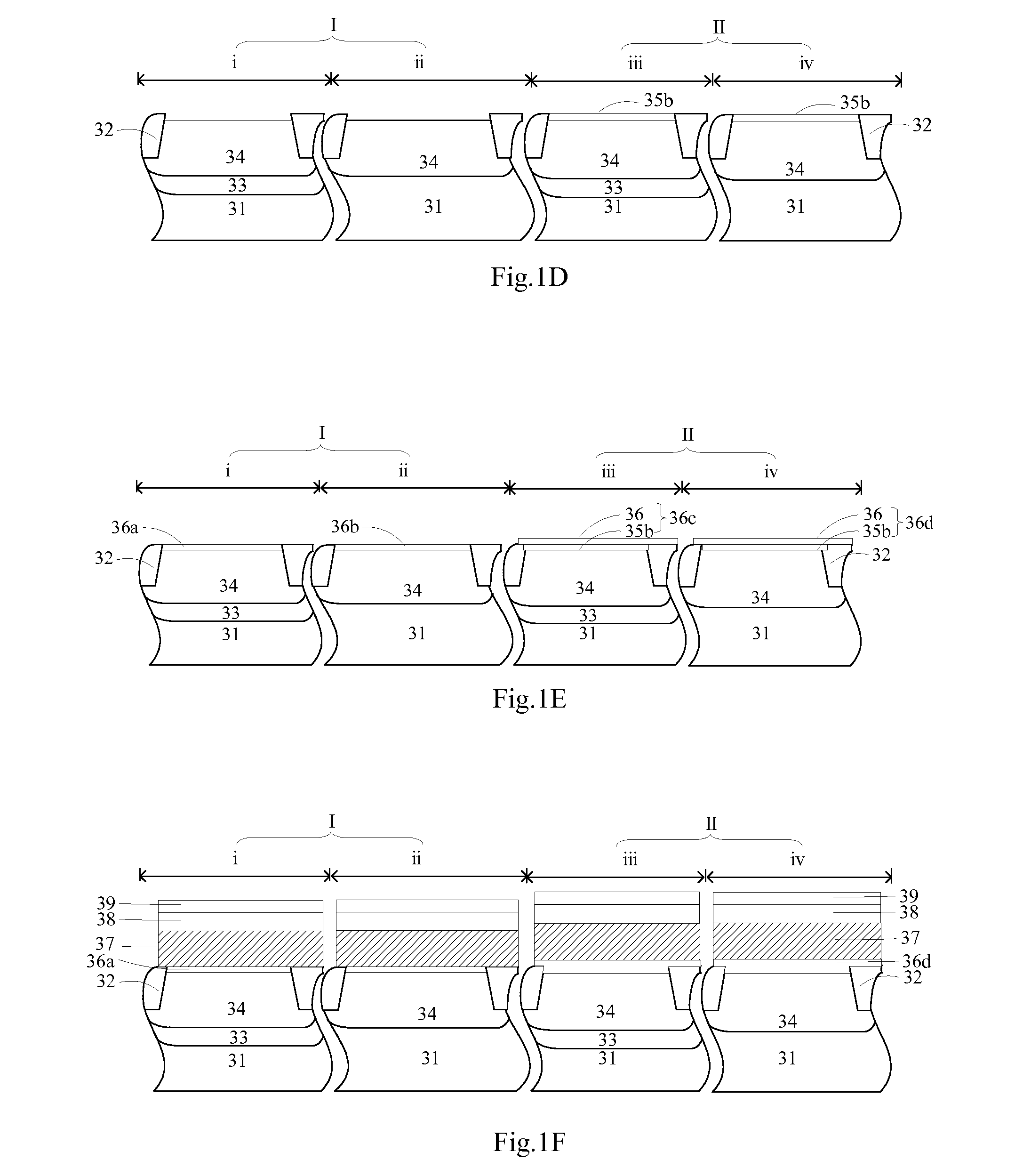
[0088]The method of fabrication of memory cells and logic transistors according to the invention is illustrated in FIGS. 2A to 2I. Referring to FIG. 2A, the semiconductor substrate 301 can be functionally divided into region I and II. Region I is a core circuit region (with thinner gate dielectric 306a and 306b) and further divided into region i, a core memory cell region, and region ii, a core logic transistor region. Region II is an IO circuit region (with thicker gate dielectric 306c and 306d) and further divided into region iii, an IO memory cell region, and region iv, an IO logic transistor region.
first embodiment
[0089]In the semiconductor substrate 301, shallow trenches 302, deep n-well regions 303 and p-well regions 304 are formed; gate dielectric layers 306a and 306b are formed in region I; gate dielectric layers 306c and 306d are formed in region II; gate structures 307a, 307b, 307c and 307d are formed respectively on the gate dielectric layers 306a and 306b in region I and the gate dielectric layers 306c and 306d in region II; and a first sidewall 401 is formed at each side of the gate structures 307a, 307b, 307c and 307d. Such a structure can be formed with reference to FIG. 1A to FIG. 1H in connection with the
[0090]The gate dielectric layers 306a, 306b, 306c and 306d are made of a high-k dielectric material, such as HfO2, Al2O3, La2O3, HfSiON or HfAlO2. Charge traps 501 are contained in the high-k dielectric layer, and are formed in the deposition process for the high-k dielectric layer. The charge traps 501 in the gate dielectric layers 306a, 306b, 306c and 306d can capture charges a...
third embodiment
[0112]The method of fabrication MOS transistors according to the invention is illustrated in FIG. 3A to 3C. Referring to FIG. 3A, shallow trenches 12 for isolating active devices electrically are formed on a semiconductor substrate 11, then a deep n-well region 13 and a p-well region 14 are formed. Next, a gate dielectric layer 15 is formed on the p-well 14 in the semiconductor substrate 11. The gate dielectric layer 15 is a high-k dielectric layer, such as HfO2, Al2O3, La2O3, HfSiON or HfAlO2, with inherent charge traps 16 therein, that is, the gate dielectric layer 15 has charge traps in it.
[0113]Referring to FIG. 3B, a gate structure 17 and a silicon oxide layer 18 are formed on the gate dielectric layer 15, then a first sidewall 19 is formed at each side of the gate structure 17, and next, source / drain extension regions 20 are formed at each side of the gate structure 17 in the semiconductor substrate 11 by ion implantation, where the implanted ions are arsenic, antimony, phosph...
PUM
 Abstract
Description
Claims
Application Information