Method and system for measuring signal characteristics of data signals transmitted between integrated circuit chips

a technology of integrated circuit chips and data signals, applied in the direction of noise figure or signal-to-noise ratio measurement, instruments, horology, etc., can solve the problems of longer off-chip communication paths, more discontinuities, and high noise, and achieve the effect of reducing the area required for implementation

Active Publication Date: 2008-06-19
IBM CORP
View PDF2 Cites 16 Cited by
  • Summary
  • Abstract
  • Description
  • Claims
  • Application Information

AI Technical Summary

Benefits of technology

[0034]The off-chip processing generates a new time base for the acquired data using a time base algorithm modified to incorporate the counter values. The time base allows various signal characteristics to be generated. The method of the present invention retains all the benefits of previous asynchronous sampling methods while drastically reducing the area required for implementation. As a result the amount of data analyzed is no longer limited by the size of on-chip data acquisition memory.

Problems solved by technology

Off-chip communication paths are longer, have higher noise, impedance mismatches, and have more discontinuities than on-chip communication paths.
When using inter-chip high-speed signaling, noise and coupling between signal lines (crosstalk) affects signal quality.
Transmission line systems are characterized by noise, propagation speed, losses, and reflections due to imperfect terminations.
This is done using the scope time base and may lead to increased apparent jitter on the displayed signal due to weaknesses in the time base circuitry.
Long runs of identical characters provide no transitions to trigger from and so a complete eye diagram is almost impossible to achieve.
This is a useful absolute measure but might not properly represent the jitter “seen” by a real system if the receiver also uses clock recovery to track the data to remove jitter.
Error testing will provide an overall measure of how well a system is performing but does little to help in understanding the underlying causes for lower that expected performance.
This would result in a “high information depth.” However, eye diagrams are typically composed of voltage / time samples of the original data that are acquired at some sample rate that may be orders of magnitude slower that the actual data rate.
This means that the eye diagrams so acquired would be “information shallow.”
This becomes a problem when issues arise that occur infrequently.
Modern computer systems can have hundreds of communication channels per die, making it impractical to view the eye diagram of each individual channel using external test equipment.
However, distribution of a high speed synchronous trigger signal across hundreds of channels is impractical.
In modern CMOS processes, it is exceptionally difficult to realize a delay line with both fine resolution (i.e., less than an inverter delay—a few picoseconds) and with a large delay range (hundreds of picoseconds).
Delay lines often have poor accuracy, high power dissipation and large area, making them impractical for use on a per-channel bases.

Method used


Image

  • Method and system for measuring signal characteristics of data signals transmitted between integrated circuit chips
  • Method and system for measuring signal characteristics of data signals transmitted between integrated circuit chips
  • Method and system for measuring signal characteristics of data signals transmitted between integrated circuit chips

Examples


Embodiment Construction

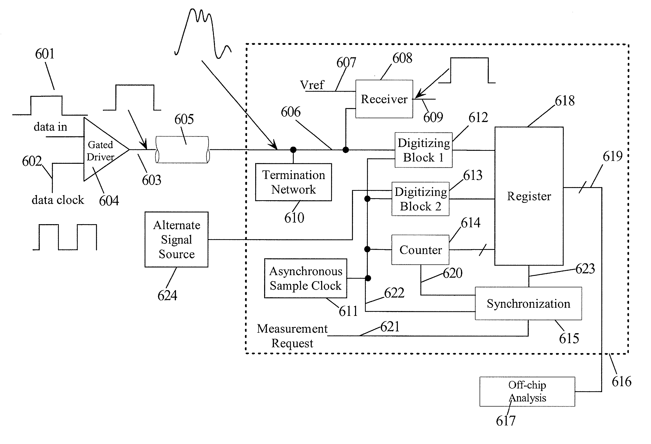
[0051]In the following description, numerous specific details are set forth to provide a thorough understanding of the present invention. However, it will be obvious to those skilled in the art that the present invention may be practiced without such specific details. In other instances, well-known circuits may be shown in block diagram form in order not to obscure the present invention in unnecessary detail. For the most part, details concerning timing considerations and the like have been omitted inasmuch as such details are not necessary to obtain a complete understanding of the present invention and are within the skills of persons of ordinary skill in the relevant art.

[0052]An explanation of how timing jitter of a eye pattern used in embodiments of the present invention may be determined is found in the publication: “Firmware Measurement Algorithms for HP 83480 Digital Communications Analyzer”, Hewlett-Packard Journal, 1996, which is hereby incorporated by reference herein.

[005...


PUM


Abstract

Data signals received in an integrated circuit are coupled to a receiver and to an on-chip data acquisition system which takes measurement samples of the data signal in response to a measurement request. The measurement request is synchronized with an asynchronous sample clock signal generating a capture signal and a counter reset signal. A counter measures the number of sample clock cycles between measurement requests. On receipt of a measurement request, the capture signal triggers the storage, as capture data, the preset number of cycles in the counter and the measurement samples in a register. The counter is synchronously reset and the capture data is sent to off-chip storage. The off-chip storage stores an arbitrary amount of capture data and the area on-chip is greatly reduced for the on-chip data acquisition. An off-chip analysis is used to construct an effective time base for the capture data for signal analysis

Description

CROSS REFERENCE TO RELATED APPLICATION[0001]The present invention is related to the following U.S. patent application which is incorporated by reference:[0002]Ser. No. 11 / 427,860 (Attorney Docket No. AUS920060202US1) filed Jun. 30, 2006 and entitled “Method And Apparatus for Constructing a Synchronous Signal Diagram From Asynchronously Sampled Data”.TECHNICAL FIELD[0003]The present invention relates in general to board level transmission line drivers and receivers, and in particular, to methods of testing data channels transmitting data between integrated circuits driving transmission lines coupling elements on circuit boards.BACKGROUND INFORMATION[0004]Digital computer systems have a history of continually increasing the speed of the processors used in the system. As computer systems have migrated towards multiprocessor systems, sharing information between processors and memory systems has also generated a requirement for increased speed for the off-chip communication networks. Des...

Claims


Application Information

Patent Timeline
Patent Type & Authority Applications(United States)
IPC IPC(8): G01R13/02G01R29/26
CPCG01R31/3016G01R31/31727G01R31/31725
Inventor GEBARA, FADI H.SCHAUB, JEREMY D.
Owner IBM CORP
Why Eureka
Try Eureka