Laser optical system

a laser optical system and laser technology, applied in the field of laser optical systems, can solve the problems of limiting productivity and high maintenance costs, and achieve the effects of reliable operation, simple design, and compact siz

Inactive Publication Date: 2008-06-26
UVTECH SYST
View PDF38 Cites 38 Cited by
  • Summary
  • Abstract
  • Description
  • Claims
  • Application Information

AI Technical Summary

Benefits of technology

[0008]The present invention was made in light of the above needs and problems, and is directed to an apparatus and method for laser exposure on a surface. Accordingly, it is an exemplified feature of the present invention to provide a laser optical system and method that is simple in design, compact in size, reliable in operation, and with a low cost of ownership. It is a further feature of the invention to provide a laser optical system that can be configured into multiple optical configurations to permit operation at multiple wavelengths and processing of different applications with a single system. It is still another feature of the invention to precisely deposit laser radiation uniformly on the surface of the substrate, and create a reaction without depositing high thermal energy into the bulk of the film. Another feature of the invention is to provide a low pulse energy system with the ability to spread the laser energy sufficiently to permit the processing of damage sensitive films. Finally, it is a feature of the invention to provide relatively high productivity measured in substrates per hour.

Problems solved by technology

Prior art imaging, curing and annealing systems for semiconductor manufacturing may use large gas lasers, such as excimer lasers, that require frequent gas change, optics change, and have high maintenance costs with frequent down times that limit productivity.

Method used


Image

  • Laser optical system
  • Laser optical system
  • Laser optical system

Examples


Embodiment Construction

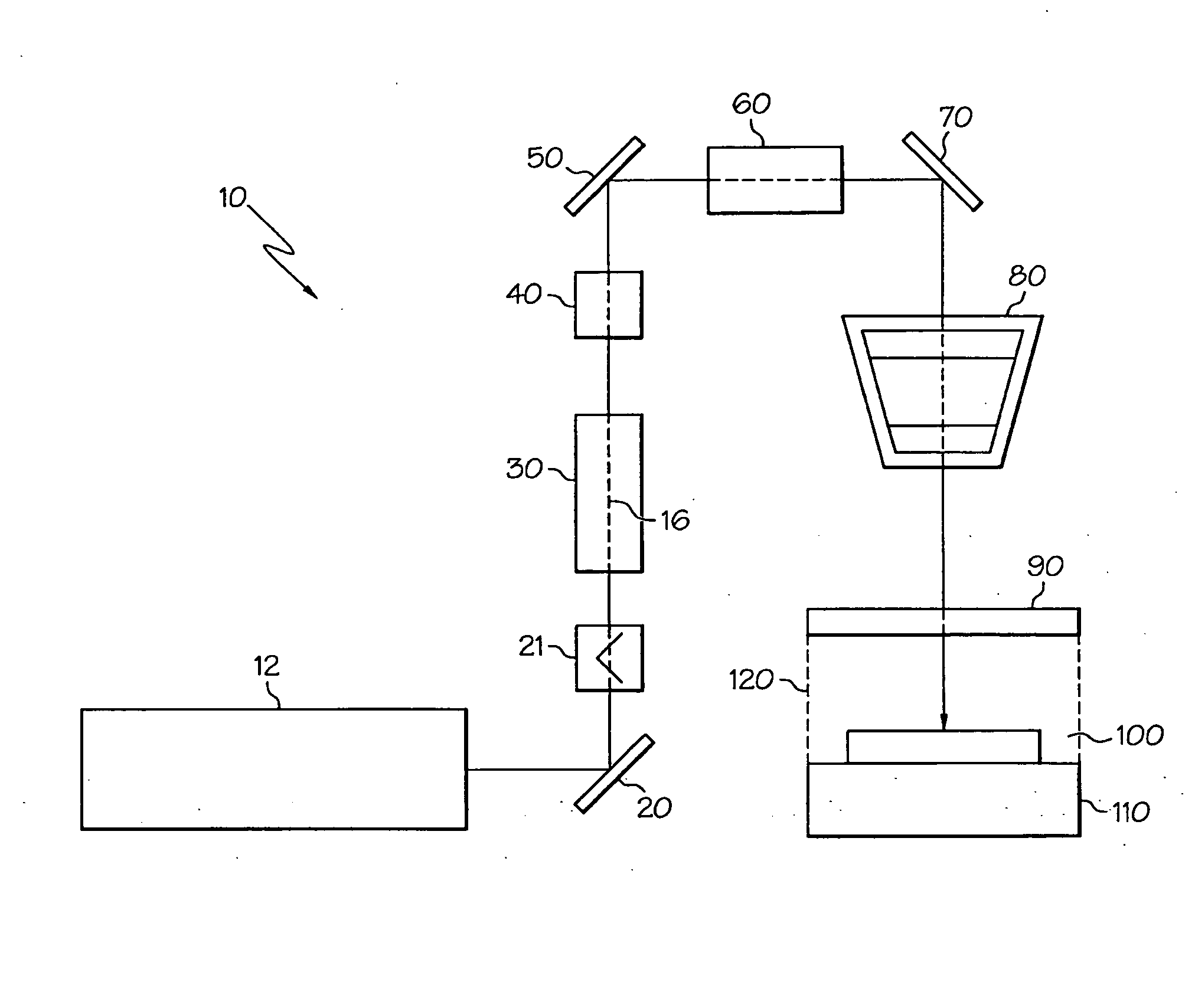
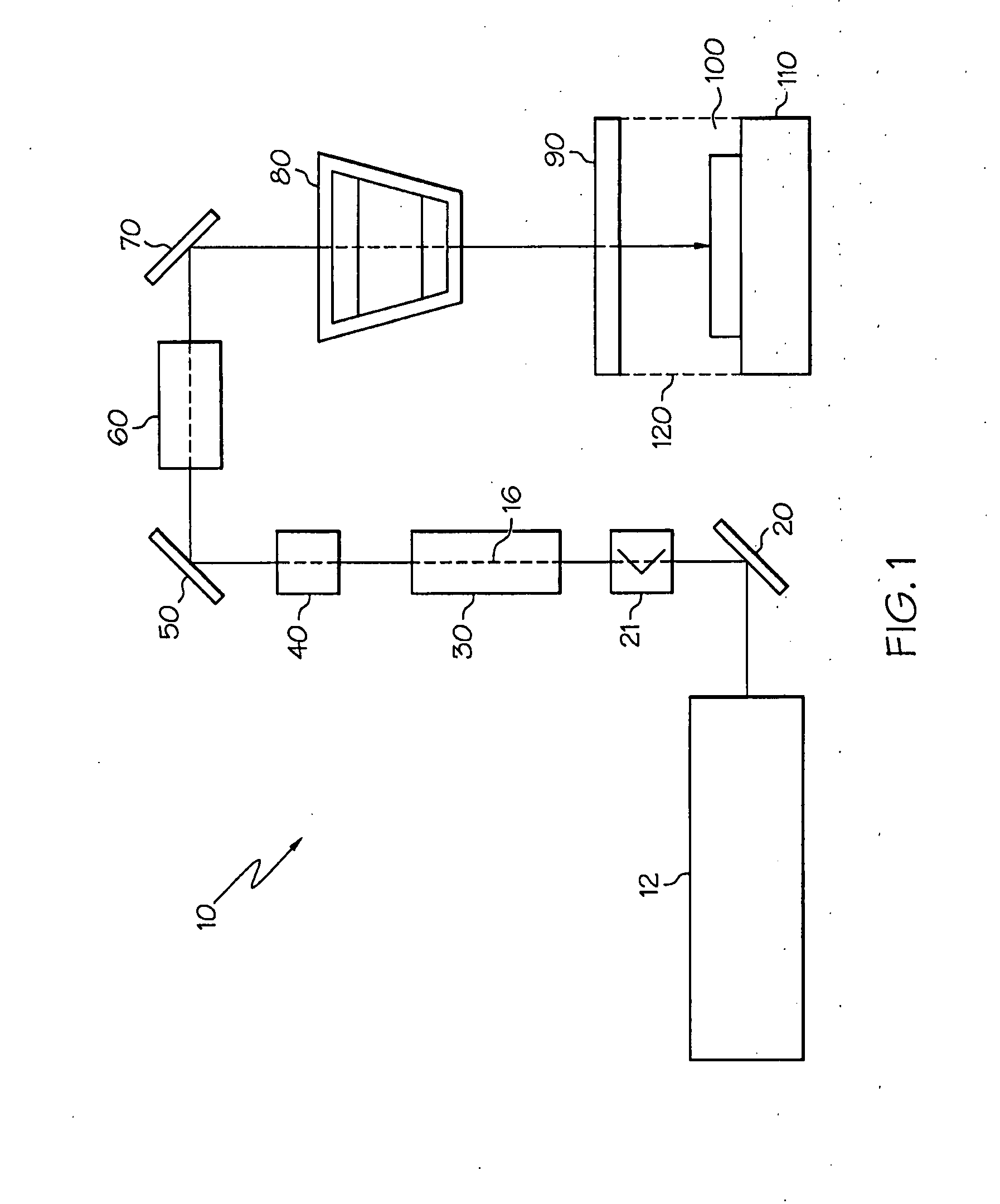
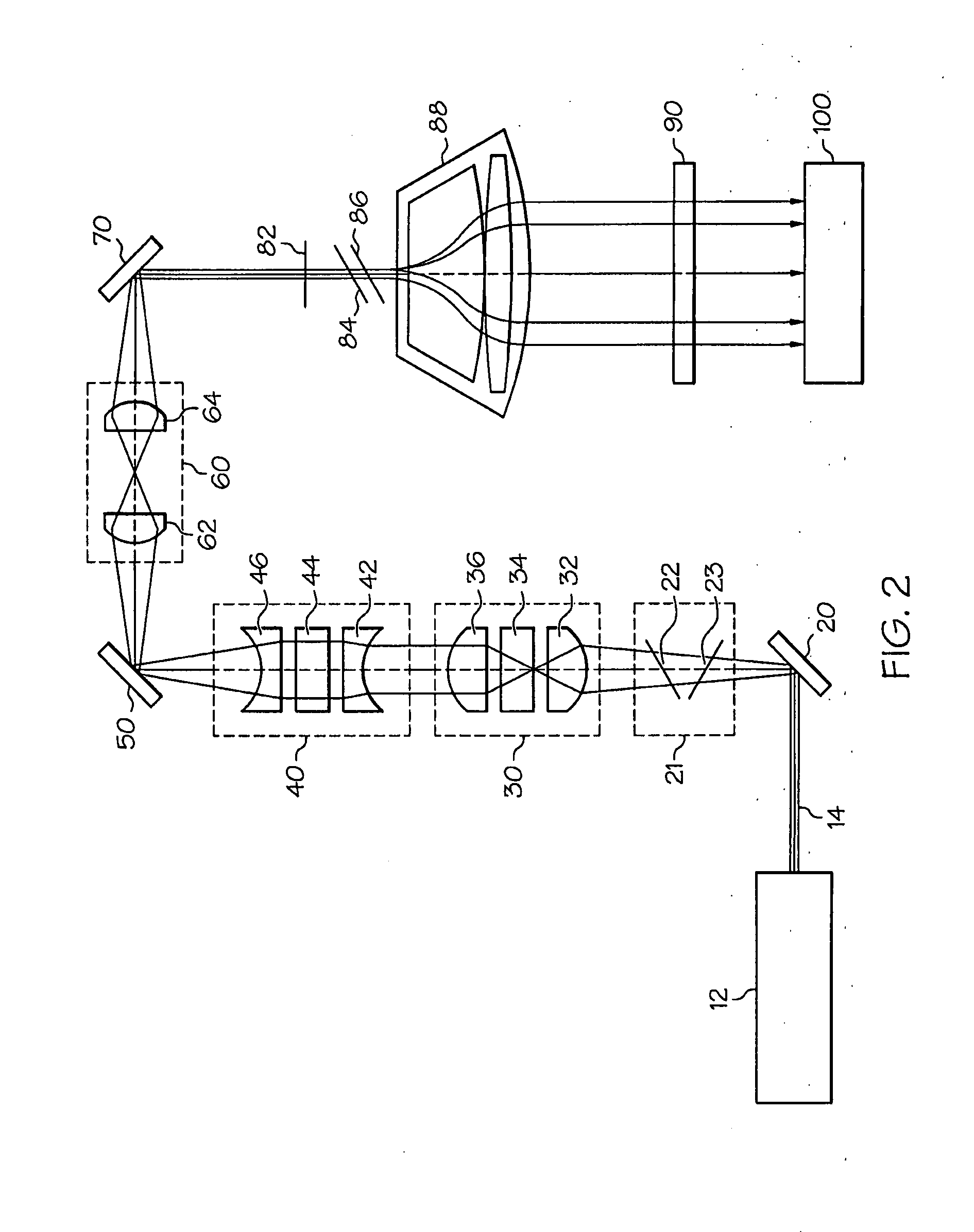
[0025]In a preferred embodiment, the laser optical system of the present invention is designed to transform a non-uniform beam of Gaussian intensity distribution into a beam of relatively uniform intensity distribution, and with a desired diameter. The uniform intensity permits wider process latitude and process control in manufacturing. This is especially useful in advanced semiconductor manufacturing. The controlled diameter beam permits optimum processing with higher throughput for cost effective manufacturing.

[0026]In the present invention, in order to achieve high uniformity of the reaction on the substrate, a beam flattener is used that removes the high intensity peak of the laser's Gaussian output beam, and re-directs the rays into a uniform distribution at the substrate plane. Further, a beam scanning, pulse-distribution approach is used that deposits the laser pulses apart from each other in both time and space dimensions, so that in a given area of the substrate, only sing...


PUM

PropertyMeasurementUnit
wavelengthaaaaaaaaaa

Abstract

A compact optical system is provided for delivering laser radiation with high optical efficiency and uniformity. The optical system includes, in order of the propagation of light, a refractive beam expander to adjust beam size and energy density, a beam flattening module to increase throughput and beam uniformity, an anamorphic corrector to equalize ray distribution in both axes, an attenuator assembly to adjust beam intensity, galvanometer mirrors to scan the beam across a substrate surface, and a focusing lens containing a plurality of refractive elements to deliver the beam at the substrate plane. The laser optical system shapes the laser source beam to increase its effective width for greater productivity in manufacturing, and reduces peak intensity to minimize substrate damage. The laser optical system design is optimized for maximum transmission and optical efficiency for low cost operation with a small laser.

Description

FIELD OF THE INVENTION[0001]The present invention relates generally to an optical system apparatus using laser light, and more specifically, a scanning laser apparatus and method for annealing, curing and imaging of semiconductor films or optical devices.BACKGROUND OF THE INVENTION[0002]The rapid increase in integrated circuit complexity, with circuit density doubling roughly every two years (following Gordon Moore's Law), has resulted in the use of thinner, easily damaged films. New high-speed thin oxides, called ‘low-k films,” are very easily damaged by conventional annealing, imaging and curing systems. Currently, these functions are performed with large-footprint, complex and high-cost tools. The increasing cost of energy also generates a need for more energy efficient radiation sources used to anneal, image, and cure coatings on semiconductor films in IC production process. There is therefore a need for a simple, low-cost-of-ownership, and energy efficient laser optical system ...

Claims


Application Information

Patent Timeline
Patent Type & Authority Applications(United States)
IPC IPC(8): H01S3/10
CPCB23K26/0807B23K2201/40B29C67/0066G02B19/0014H01L21/268G02B19/0095G02B19/0052G02B27/0955B23K26/082B29C64/135B23K2101/40
Inventor ELLIOTT, DAVID J.HARTE, KENNETH J.MILLMAN, RONALD P.CHAPLICK, VICTORIA M.
Owner UVTECH SYST
Why Eureka
Try Eureka