Enhanced mobility CMOS transistors with a v-shaped channel with self-alignment to shallow trench isolation

a technology of cmos transistor and self-alignment, which is applied in the field of complementary metal oxide semiconductor (cmos) transistors, can solve the problems of inability to use high-performance cmos devices, propensity for epitaxy defect generation, and complex processes, and achieve the effect of improving performan

Inactive Publication Date: 2008-07-24
GLOBALFOUNDRIES INC
View PDF7 Cites 177 Cited by
  • Summary
  • Abstract
  • Description
  • Claims
  • Application Information

AI Technical Summary

Benefits of technology

[0010]The present invention addresses the needs described above and provides structures and methods for an enhanced perform

Problems solved by technology

However, disadvantages of this approach include the complexity of the processes and the propensity of epitaxy for defect generation.
Furthermore, a substantial portion of the surface area around the boundary between two different crystallographic orientations becomes unusable for high performance CMOS devices due to crystalline defects at the boundary

Method used


Image

  • Enhanced mobility CMOS transistors with a v-shaped channel with self-alignment to shallow trench isolation
  • Enhanced mobility CMOS transistors with a v-shaped channel with self-alignment to shallow trench isolation
  • Enhanced mobility CMOS transistors with a v-shaped channel with self-alignment to shallow trench isolation

Examples


first embodiment

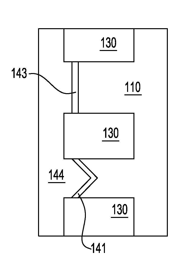
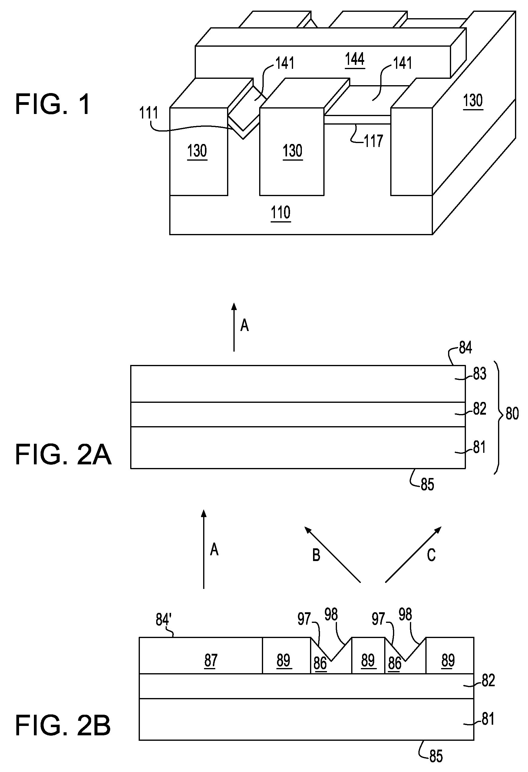
[0051]FIG. 1 shows a bird's eye view of a portion of an exemplary SRAM structure after a gate stack etch and before removal of the gate dielectric according to the present invention. In FIG. 1, a semiconductor substrate 110, shallow trench isolation 130, a gate dielectric 141, a V-shaped groove 111 formed in a PFET region, a flat semiconductor area 117 formed in an NFET region, and a gate line 144 are shown. The purpose of this bird's eye view is to show the general structure of the present invention that comprises a V-shaped groove formed by two crystallographic facets meeting at or around the middle of the semiconductor area and a channel formed adjacent to and beneath the V-shaped groove such that the direction of the current flow is in the direction of the ridge formed by the two adjoining crystallographic facets.

[0052]Before describing the present invention in further detail, definitions of terms used in this disclosure are presented herein.

[0053]The term “substrate orientation...

second embodiment

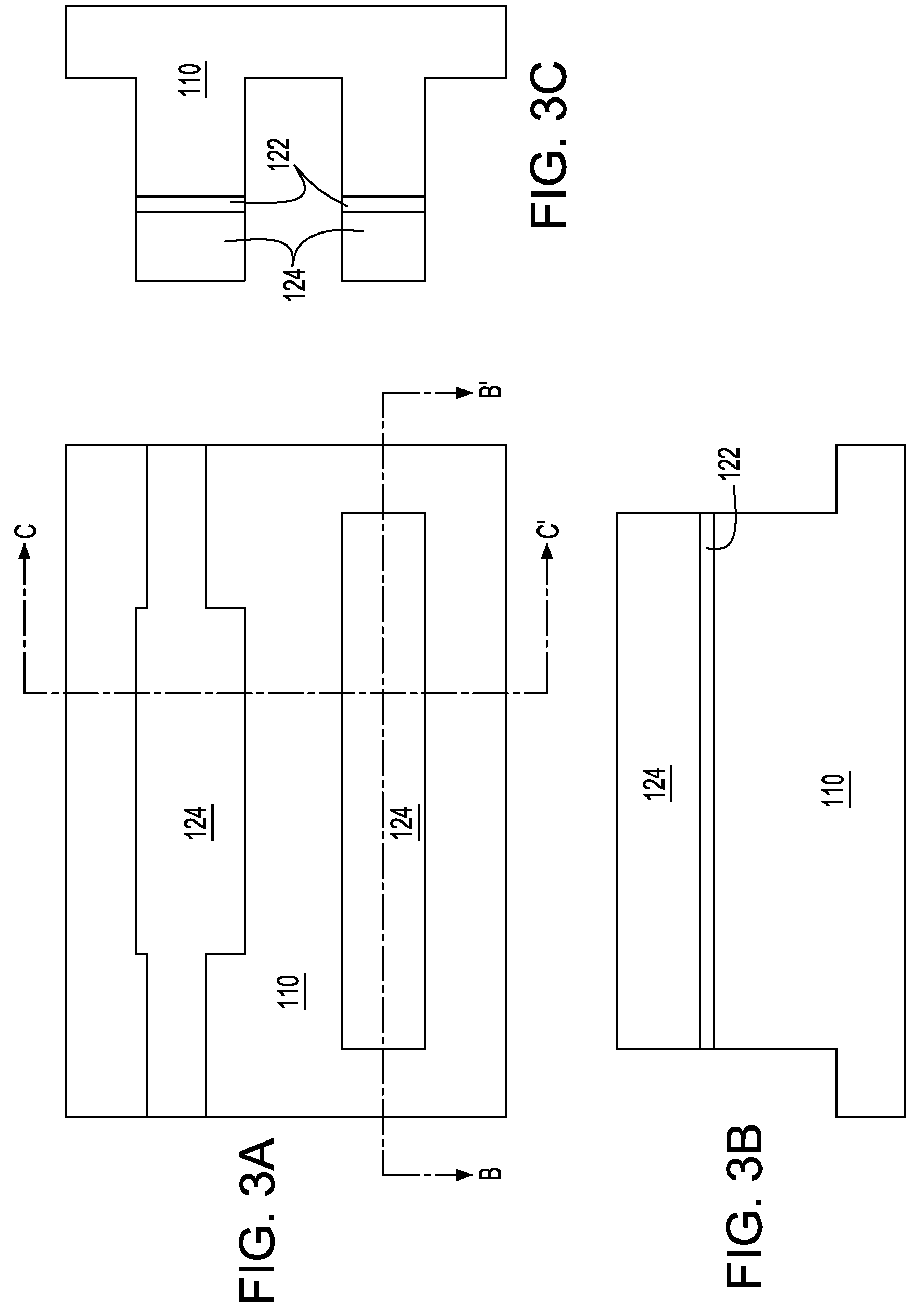
[0075]According to the present invention, identical processing steps are employed up to the lithographic patterning of shallow trench isolation (STI) and an STI etch as shown in FIGS. 3A-3C. Preferably, during the deposition of the pad nitride 124, however, a thicker pad nitride layer is deposited. The same STI fill process is used to fill the STI regions with STI material 130.

[0076]The substrate is planarized with chemical mechanical polishing (CMP) after the STI regions are filled with STI material 130. In a preferred version of the second embodiment of the present invention, however, the residual pad nitride 124′ is thicker than that in the first embodiment so that after the planarization. The surface of the pad oxide 122 is at this point recessed by the thickness of the residual pad nitride 124′ at the end of the CMP step as shown in FIGS. 9A-9C.

[0077]The residual pad nitride 124′ is removed preferably by a wet etch. An STI spacer layer 132 is deposited by blanket deposition fol...


PUM


Abstract

The present invention provides structures and methods for a transistor formed on a V-shaped groove. The V-shaped groove contains two crystallographic facets joined by a ridge. The facets have different crystallographic orientations than what a semiconductor substrate normally provides such as the substrate orientation or orientations orthogonal to the substrate orientation. Unlike the prior art, the V-shaped groove is formed self-aligned to the shallow trench isolation, eliminating the need to precisely align the V-shaped grooves with lithographic means. The electrical properties of the new facets, specifically, the enhanced carrier mobility, are utilized to enhance the performance of transistors. In a transistor with a channel on the facets that are joined to form a V-shaped profile, the current flows in the direction of the ridge joining the facets avoiding any inflection in the direction of the current.

Description

FIELD OF THE INVENTION[0001]The present invention relates to semiconductor devices, and particularly, to complementary metal oxide semiconductor (CMOS) transistors.BACKGROUND OF THE INVENTION[0002]A key metric for performance of transistors is the on-current, which is the current of a transistor per unit gate width when it is turned on. The minority carrier mobility has been identified as a limiting factor in determining the on-current of high performance transistors. One of the key parameters determining the mobility of minority carriers is the crystallographic surface orientation on which the channel of the transistor is formed. By manipulating the transistor structure such that a favorable surface orientation is used for each type of transistors, both P-type field effect transistors (PFETs) and N-type field effect transistors (NFETs) with high minority carrier mobility may be formed in a CMOS transistor circuit.[0003]In some semiconductors, electron mobility and hole mobility ach...

Claims


Application Information

Patent Timeline
IPC IPC(8): H01L29/04H01L21/306
CPCH01L21/823807H01L21/823828H01L27/11H01L27/1104H01L29/7853H01L29/1037H01L29/4236H01L29/66621H01L29/045H10B10/00H10B10/12
Inventor ZHU, HUILONGDYER, THOMAS W.
Owner GLOBALFOUNDRIES INC
Why Eureka
Try Eureka