Solderable layer and a method for manufacturing the same

a technology of soldering layer and manufacturing method, which is applied in the direction of resistive material coating, metallic material coating process, metal-working apparatus, etc., can solve the problems of unstable copper or copper alloy, degrading its solderability, environmental problems, etc., to reduce the formation rate of imcs, reduce the diffusion rate of copper, and reduce the diffusion of copper

Inactive Publication Date: 2008-07-24
CHENG YEN HANG
View PDF9 Cites 17 Cited by
  • Summary
  • Abstract
  • Description
  • Claims
  • Application Information

AI Technical Summary

Benefits of technology

[0013]The OBF can reduce diffusion of copper from the substrates into the immersion-deposited layer. Diffused copper and tin are the materials for a formation of IMC. Therefore, a reduce of copper diffusion can reduce a formation rate of the IMCs. Thus, the immersion tin coating of the present invention has a more steady solderability than a conventional immersion tin coating without OBF.

Problems solved by technology

However, copper or copper alloys are unstable and easily react with oxygen to form oxides.
Moreover, the formation of oxides can degrade its solderability.
However, the HASL that plates tin and lead on the circuit board will result in environment problems.
These whiskers could fall on any part of the circuit boards and cause serious reliability risks.
Moreover, many structural defects are produced in the coating layer.
Moreover, excess amount of IMC can degrade the solderability of immersion tin coatings.
The excessive growth of IMCs will decrease the solderability of the immersion-deposited layer.
However, the reliability of the metal chosen and IMCs of copper and the metal would need to be established over a long period of time.

Method used


Image

  • Solderable layer and a method for manufacturing the same
  • Solderable layer and a method for manufacturing the same
  • Solderable layer and a method for manufacturing the same

Examples


examples

[0046]The OBF make up solution was diluted to predetermined concentrations and on the substrate surfaces were maintained at 6 μl / cm2. The thickness of the OBF can be calculated from the ratio and density. The thickness of a 6-μl 1 wt % OBF make up solution coated on a 1-cm2 surface was calculated as 0.3 μm by using a density of 2 g / cm3 for a dry OBF. An organic buffer film (OBF) make up solution can be varied as table 1.

TABLE 1AComponent and composition of an organic buffer film (OBF)make up solution.ComponentComposition (wt %)OBF MANafion ®50PTFE25Polyaniline25OBF MBNafion ®65Polyaniline35OBF MCNafion ®100OBF MDNafion ®50Polyfuran10Poly(dibenzofuran)15Polyaniline25

TABLE 1BComponent and composition of an organic buffer film (OBF)ComponentComposition (wt %)OBF AOBF MA1Ethanol99OBF BOBF MB1Ethanol99OBF COBF MC1Ethanol99OBF DOBF MD1Ethanol99OBF EOBF MA5Ethanol95OBF FOBF MA10Ethanol90

[0047]A solution with immersed tin can be varied as table 2.

TABLE 2Components and compositions of soluti...

example 1

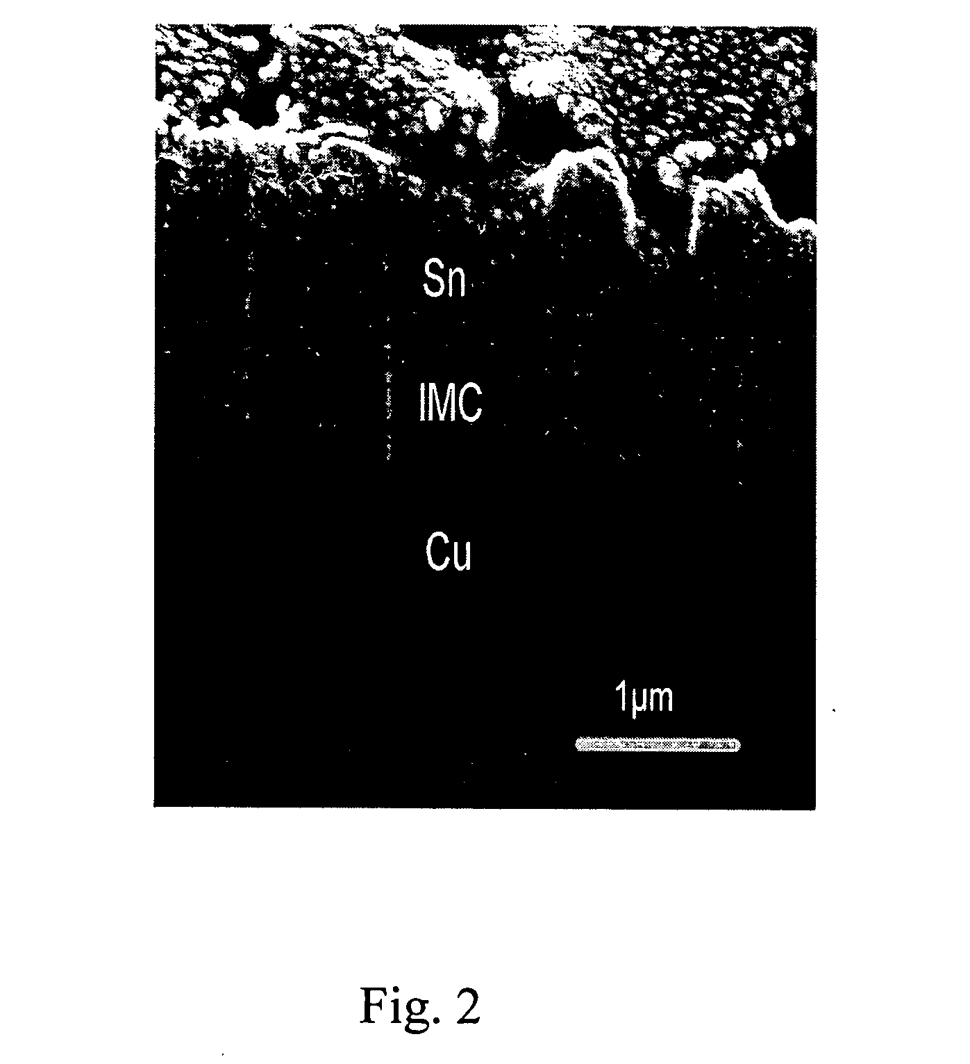
[0053]The OBF MA was diluted with ethanol to 1% and coated on copper circuitries in circuit board to form modified surface of circuitries. Then dipped the modified circuit board in the immersion plating solution A for 15 minutes at 70° C. and an immersion tin coating was deposited on circuitries in circuit board. The immersion tin coating has a thickness of 1.7 μm. According to the scanning electronic microscope (SEM), The grains sizes of the coating surface were about 1.5˜3 μm and no whiskers were found after 240 hours storage at room temperature.

example 2

[0054]The OBF MA was diluted with ethanol to 5% and coated on copper circuitries in circuit board to form modified surface of circuitries. Then dipped the modified circuit board in the immersion plating solution A for 15 minutes at 70° C. and an immersion tin coating was deposited on circuitries in circuit board. The immersion tin coating has a thickness of 0.97 μm. According to the scanning electronic microscope (SEM), The grains sizes of the coating surface were about 1.7˜3.2 μm and no whiskers were found after 240 hours storage at room temperature.


PUM

PropertyMeasurementUnit
thicknessaaaaaaaaaa
temperatureaaaaaaaaaa

Abstract

A solderable layer has an organic buffer film (OBF) and an immersion tin coating deposited on a substrate. The OBF is first coated on the surface of the substrate to modify the surface of the substrate and having fluorocarbon-based polymers (solution type). The immersion plating solution pass through the OBF and the immersion tin coating is then coated on the substrate. A method to manufacture the solderable layer according to any one of claims 1 to 12 has following steps of (1) coating an organic buffer film (OBF) on a surface of a substrate to form a modified surface, (2) drying the modified surface, (3) applying the substrate into a solution with immersed tin compositions to allow the immersed tin to deposit on the modified surface, (4) rinsing the modified surface with water and (5) drying the substrate.

Description

BACKGROUND OF THE INVENTION[0001]1. Field of Invention[0002]The present invention relates to a solderable layer and a method for manufacturing the same, and more particularly to a solderable layer including an organic buffer film and an immersed-tin layer on a substrate and a method for manufacturing the solderable layer. The solderable layer has a steady solderability and eliminates tin whiskers from forming on a surface of the immersed-tin layer.[0003]2. Description of the Related Art[0004]Circuit boards, such as printed circuited board (PCB) are generally fabricated in a surface-finished condition by board manufacturers and are shipped to an assembly house. Some circuitry is left exposed for later soldering and hence the exposed circuitry must retain a good solderability. The exposed circuitry is composed of copper or copper alloys. However, copper or copper alloys are unstable and easily react with oxygen to form oxides. Moreover, the formation of oxides can degrade its solderab...

Claims


Application Information

Patent Timeline
Patent Type & Authority Applications(United States)
IPC IPC(8): B32B33/00B05D5/12
CPCB23K1/08B23K2201/42H05K3/244Y10T428/12556H05K2201/015H05K2203/073H05K3/282B23K2101/42
Inventor CHENG, YEN-HANG
Owner CHENG YEN HANG
Why Eureka
Try Eureka