Combined Etching and Doping Media for Silicon Dioxide Layers and Underlying Silicon

a technology of silicon dioxide and underlying silicon, which is applied in the direction of sustainable manufacturing/processing, final product manufacturing, other domestic articles, etc., can solve the problems of space-charge region breakage and voltage increase, and achieve the effect of high etch rate and facilitate targeted phosphorus doping

Inactive Publication Date: 2008-09-04
MERCK PATENT GMBH
View PDF8 Cites 28 Cited by
  • Summary
  • Abstract
  • Description
  • Claims
  • Application Information

AI Technical Summary

Benefits of technology

[0027]The object of the present invention is therefore to provide a suitable etching medium with the aid of which silicon dioxide layers of solar cells can be etched selectively at high etch rates. A further object of the present invention is there

Problems solved by technology

On input of photon energy into the solar cell (sunlight), charge carriers are formed at this p-n

Method used


Image

  • Combined Etching and Doping Media for Silicon Dioxide Layers and Underlying Silicon
  • Combined Etching and Doping Media for Silicon Dioxide Layers and Underlying Silicon
  • Combined Etching and Doping Media for Silicon Dioxide Layers and Underlying Silicon

Examples


example 1

[0078]Preparation and Composition of the Paste

[0079]6 g of Aerosil 200 (Degussa-Huels AG) were stirred into 100 g of 85% ortho-phosphoric acid (Merck Art. 1.00573) with stirring. The resultant paste was stirred using a paddle stirrer for a further 20 min.

example 2

[0080]Preparation and Composition of the Paste

[0081]3% by weight of PVP K90 were stirred into a mixture of 48.5% by weight of H3PO4 (85%) and 48.5% by weight of 1-methyl-2-pyrrolidone. The resultant paste was stirred using a paddle stirring for a further 20 min.

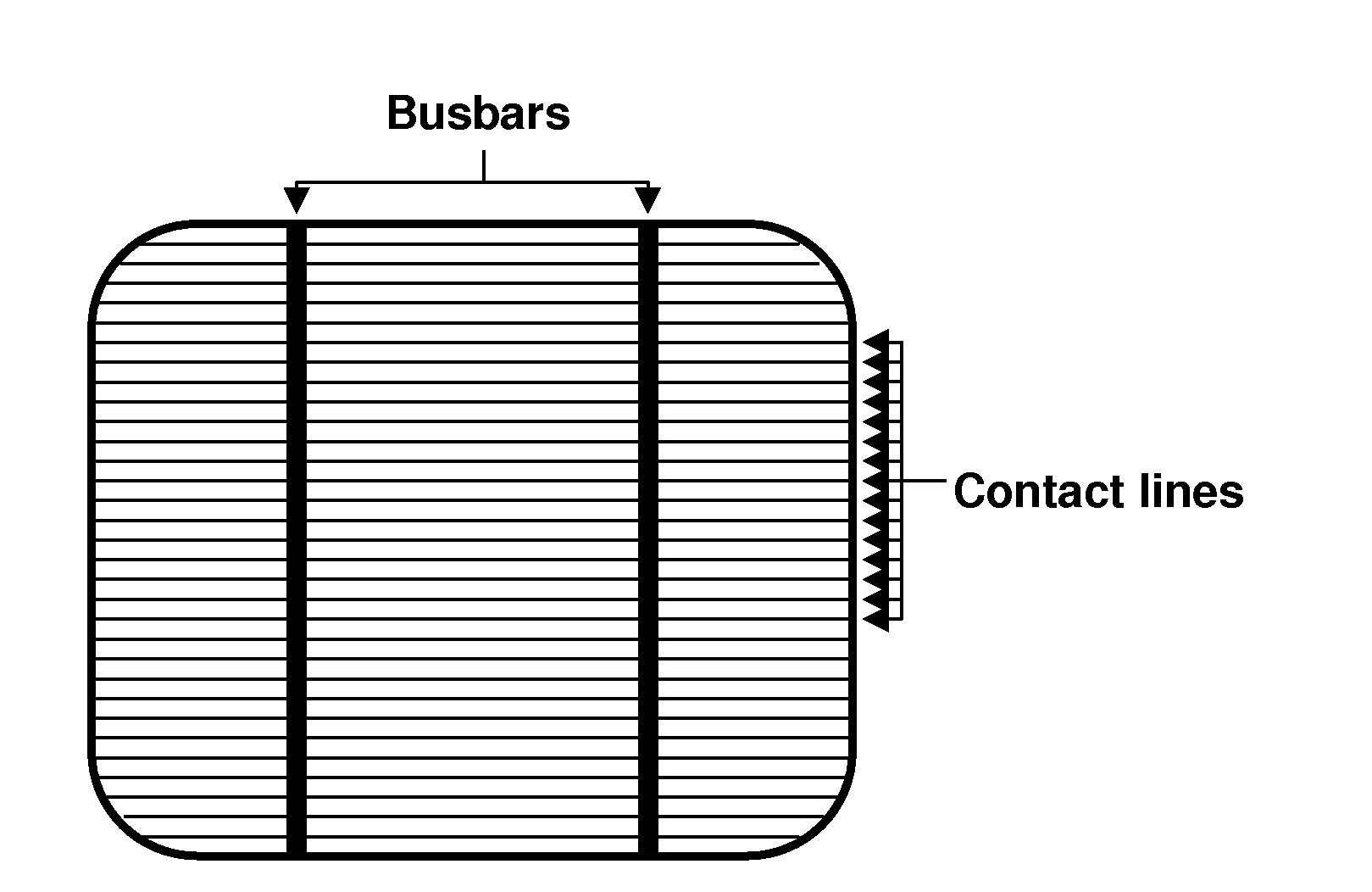
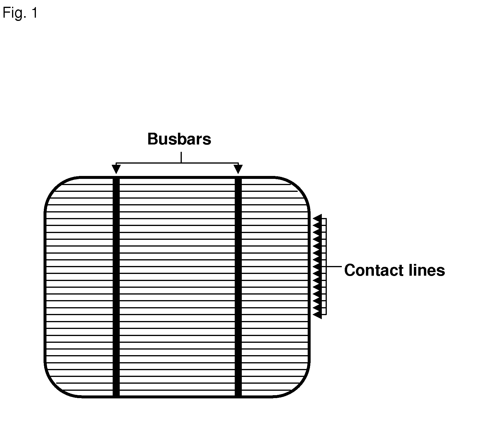
[0082]An etching paste prepared in the manner described is printed on a commercially available screen-printing machine using a type 120 T polyester screen. The layout shown in FIG. 1 is imaged on the screen and transferred onto the substrate. The substrate employed is a polycrystalline solar cell having a size of 100×100 mm2 with a full-area silicon dioxide passivation layer. Immediately after printing, the substrate is heated on a hotplate at 300° C. for 100 seconds. Complete etching-through of the silicon dioxide layer is visually evident after only about 60 seconds. The substrate is then introduced into a diffusion oven containing atmospheric air at 850° C. for 30 min.

[0083]After removal of the phosphorus glass layer, the ...


PUM

PropertyMeasurementUnit
Temperatureaaaaaaaaaa

Abstract

The present invention relates firstly to HF/fluoride-free etching and doping media which are suitable both for the etching of silicon dioxide layers and also for the doping of underlying silicon layers. The present invention also relates secondly to a process in which these media are employed.

Description

[0001]The present invention relates firstly to HF / fluoride-free etching and doping media which are suitable both for the etching of silicon dioxide layers and also for the doping of underlying silicon layers. The present invention also relates secondly to a process in which these media are employed.PRIOR ART AND OBJECT OF THE INVENTION [0002]The term “solar cell” below is defined as mono- and polycrystalline silicon solar cells, independently of solar cell types based on other materials.[0003]The mode of action of a solar cell is based on the photoelectric effect, i.e. on the conversion of photon energy into electrical energy.[0004]For silicon solar cells, pre-doped silicon base material (usually p-doped Si) is to this end doped with opposite charge carriers with a different name (for example phosphorus doping results in n+ conduction), i.e. a p-n junction is produced.[0005]On input of photon energy into the solar cell (sunlight), charge carriers are formed at this p-n junction, whi...

Claims


Application Information

Patent Timeline
IPC IPC(8): H01L31/00C03C15/00
CPCC03C17/23C03C17/3411C03C2218/33Y02E10/547C09K13/06H01L31/1804C09K13/04Y02P70/50H01L21/225C03C15/00
Inventor KUEBELBECK, ARMINSTOCKUM, WERNER
Owner MERCK PATENT GMBH
Why Eureka
Try Eureka