Light emitting diode, method for manufacturing light emitting diode, integrated light emitting diode, method for manufacturing integrated light emitting diode, light emitting diode backlight, light emitting diode illumination device, light emitting diode display, electronic apparatus, electronic device, and method for manufacturing electronic device

Inactive Publication Date: 2008-09-04
SONY CORP
View PDF8 Cites 49 Cited by
  • Summary
  • Abstract
  • Description
  • Claims
  • Application Information

AI Technical Summary

Benefits of technology

[0057]In the embodiments having the above-described configurations, the first metal film composed mainly of silver is covered by the second metal film composed mainly of palladium and/or platinum, which can substantially completely prevent the migration of silver not only at room temperatures but also at high temperatures (e.g., 300° C. or higher). This can prevent the occurrence of voids (gaps arising from movement out of silver) and whiskers, which cause deterioration of the reliability of the electrode. Furthermore, oxidation and sulfuration of the first metal film can also be effectively prevented. In addition, even if a layer containing a metal that easily diffuses such as tin or gold is formed above the second metal film, reaction between the layer and the first metal film through silver migration can be prevented.
[0058]According to the embodiments of the present invention, deterioration of the

Problems solved by technology

According to the knowledge of the present inventors, however, it is difficult for the structure proposed in Patent Document 1 to prevent the migration of Ag although the surface of an Ag electr

Method used


Image

  • Light emitting diode, method for manufacturing light emitting diode, integrated light emitting diode, method for manufacturing integrated light emitting diode, light emitting diode backlight, light emitting diode illumination device, light emitting diode display, electronic apparatus, electronic device, and method for manufacturing electronic device
  • Light emitting diode, method for manufacturing light emitting diode, integrated light emitting diode, method for manufacturing integrated light emitting diode, light emitting diode backlight, light emitting diode illumination device, light emitting diode display, electronic apparatus, electronic device, and method for manufacturing electronic device
  • Light emitting diode, method for manufacturing light emitting diode, integrated light emitting diode, method for manufacturing integrated light emitting diode, light emitting diode backlight, light emitting diode illumination device, light emitting diode display, electronic apparatus, electronic device, and method for manufacturing electronic device

Examples


Example

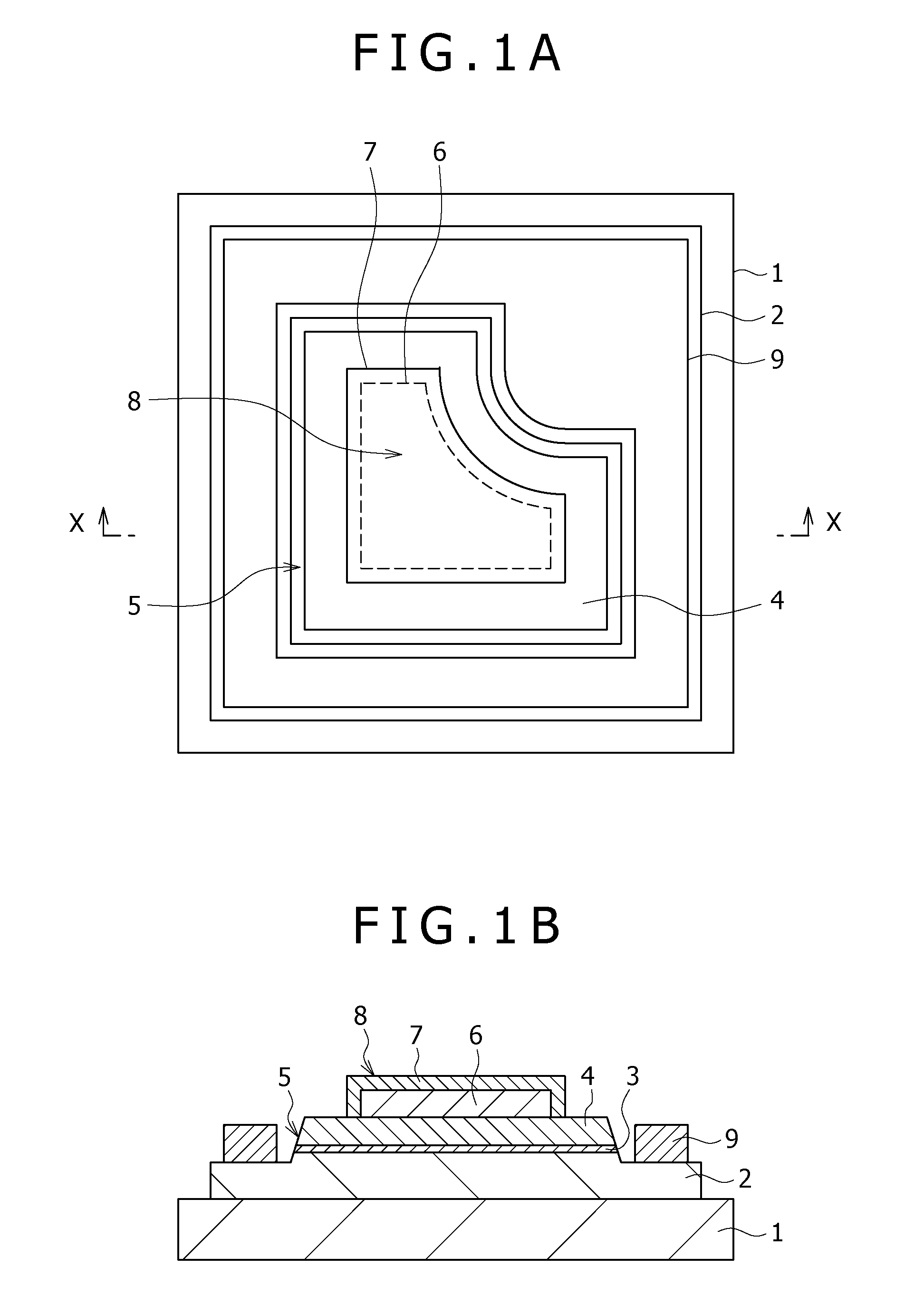
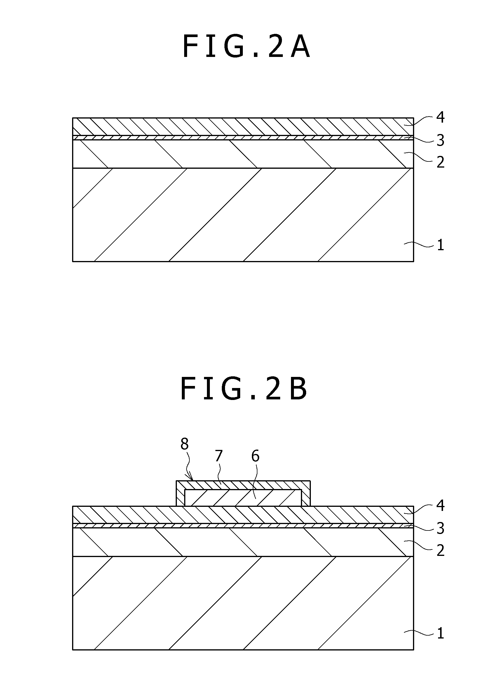
[0095]FIGS. 1A and 1B show a light emitting diode according to a first embodiment of the present invention. FIG. 1A is a plan view, and FIG. 1B is a sectional view along line X-X in FIG. 1A. This light emitting diode employs a nitride III-V compound semiconductor such as GaN.

[0096]As shown in FIGS. 1A and 1B, in the light emitting diode, an n-type nitride III-V compound semiconductor layer 2, an active layer 3 formed of a nitride III-V compound semiconductor, and a p-type nitride III-V compound semiconductor layer 4 are sequentially deposited over a substrate 1 that has one flat major face and is composed of a material transmissive for light of the emission wavelength. Any of the above-described materials can be used for the substrate 1 for example. Specifically, the substrate 1 is e.g. a sapphire substrate and the major face thereof is e.g. the c-plane. Upper part of the n-type nitride III-V compound semiconductor layer 2, the active layer 3, and the p-type nitride III-V compound s...

Example

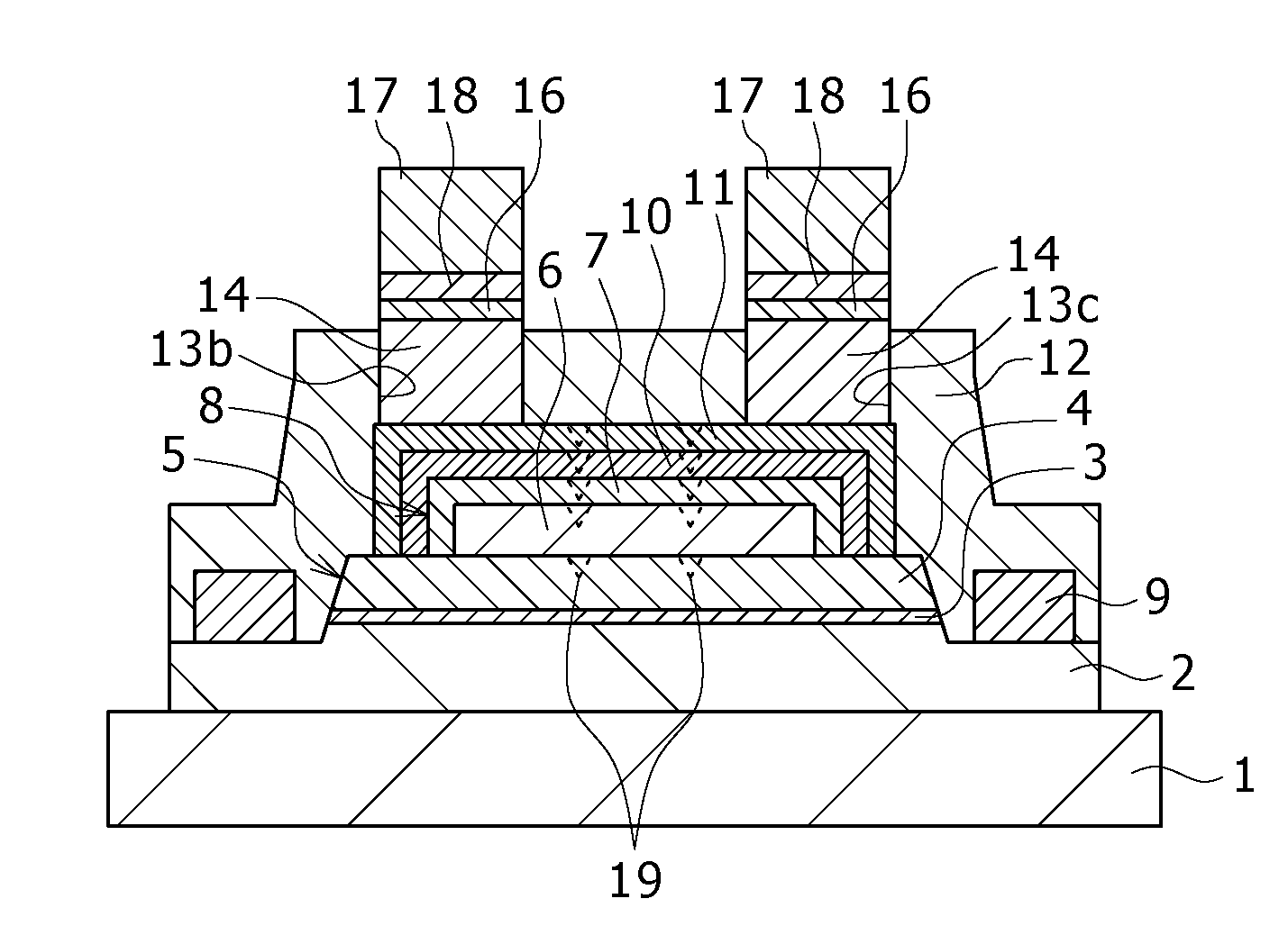
[0113]A light emitting diode according to a second embodiment of the present invention will be described below. FIG. 6 shows this light emitting diode.

[0114]As shown in FIG. 6, in this light emitting diode, a third metal film 10 composed of W, Mo, Ti, TiW, TiMo, WMo, or TiWMo is formed to cover a p-electrode 8. Furthermore, a fourth metal film 11 composed of a metal having resistance to dry etching such as Ni is formed to cover the third metal film 10. Specifically, the third metal film 10 is e.g. a TiW film formed by sputtering and having a thickness of 120 nm, and the fourth metal film 11 is e.g. a Ni film formed by sputtering and having a thickness of 50 nm. Other components of this light emitting diode are the same as those of the light emitting diode of the first embodiment.

[0115]The manufacturing method for this light emitting diode is the same as that for the first embodiment, except that the third and fourth metal films 10 and 11 are formed subsequently to formation of the s...

Example

[0117]A light emitting diode according to a third embodiment of the present invention will be described below. FIGS. 7A and 7B show this light emitting diode. FIG. 7A is a plan view, and FIG. 7B is a sectional view along line Y-Y in FIG. 7A.

[0118]As shown in FIGS. 7A and 7B, this light emitting diode includes an insulating film 12 that is formed to cover a fourth metal film 11, the side face of a mesa portion 5, the surface of an n-type nitride III-V compound semiconductor layer 2 other than the mesa portion 5, and an n-electrode 9. At least lower part of the insulating film 12 is formed of a silicon nitride film. This silicon nitride film encompasses a stoichiometric Si3N4 film formed by low-pressure CVD or the like, and a non-stoichiometric SiN film formed by plasma CVD or the like. Specifically, the insulating film 12 is formed of e.g. a silicon nitride film and a silicon oxide film on the silicon nitride film. The thicknesses of the lower silicon nitride film and the upper silic...


PUM


Abstract

Disclosed herein is a light emitting diode includes: a first semiconductor layer of a first conductivity type; an active layer on the first semiconductor layer; a second semiconductor layer of a second conductivity type on the active layer; a first electrode configured to be electrically coupled to the first semiconductor layer; and a second electrode configured to be provided on the second semiconductor layer and be electrically coupled to the second semiconductor layer, the second electrode including a first metal film that has a predetermined shape and is composed mainly of silver and a second metal film that covers the first metal film and is composed mainly of palladium and/or platinum.

Description

CROSS REFERENCES TO RELATED APPLICATIONS[0001]The present invention contains subject matter related to Japanese Patent Application JP 2006-001537 filed in the Japanese Patent Office on Jan. 6, 2006, the entire contents of which being incorporated herein by reference.BACKGROUND OF THE INVENTION[0002]1. Field of the Invention[0003]The present invention relates to a light emitting diode, a method for manufacturing a light emitting diode, an integrated light emitting diode, a method for manufacturing an integrated light emitting diode, a light emitting diode backlight, a light emitting diode illumination device, a light emitting diode display, an electronic apparatus, an electronic device, and a method for manufacturing an electronic device. The present invention can be suitably applied to e.g. light emitting diodes employing a nitride III-V compound semiconductor and various kinds of devices and apparatuses employing this light emitting diode.[0004]2. Description of the Related Art[000...

Claims


Application Information

Patent Timeline
IPC IPC(8): H01L33/00H01L33/32H01L21/28H01L33/36H01L33/40
CPCF21K9/00H01L21/0242H01L21/02433H01L21/02458H01L21/0254H01L21/0262H01L2933/0016H01L21/02647H01L33/007H01L33/08H01L33/40H01L33/405H01L21/02639H01L2224/48091H01L2224/48465H01L2924/00014H01L2924/00
Inventor WATANABE, YOSHIAKIHINO, TOMONORI
Owner SONY CORP
Why Eureka
Try Eureka