

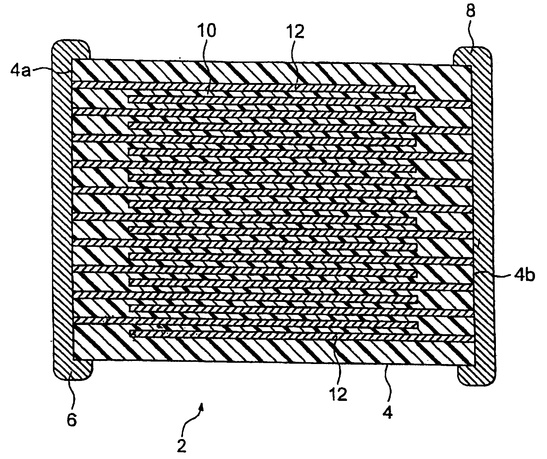
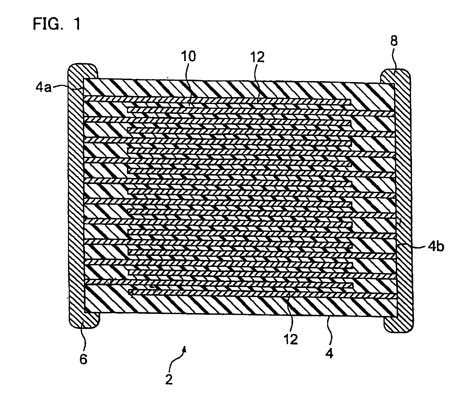
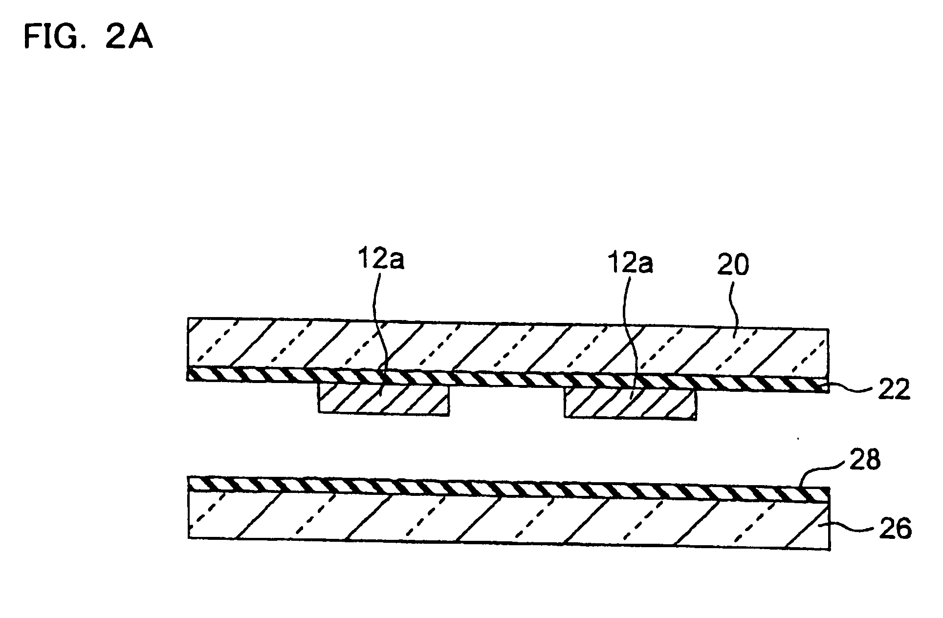
Electronic device and manufacturing method thereof
a manufacturing method and technology of electronic devices, applied in the direction of variable capacitors, fixed capacitor details, fixed capacitors, etc., can solve the problems of insufficient sintering of dielectric powder, lower melting point of ni (internal electrode layer sintering temperature), and increased cost of multilayer ceramic capacitors using precious metals. , to achieve the effect of reducing capacitance, cracking and peeling of internal electrode layers, and preventing ir deterioration
- Summary
- Abstract
- Description
- Claims
- Application Information
AI Technical Summary
Benefits of technology
Problems solved by technology
Method used
Image

Examples
example 1
[0114]First, by CVD method, the conductive material (alloy powder) of internal electrode layer was manufactured. As for the conductive material source, Ni chloride and Re chloride was used. The Crucible introduced with Ni chloride and the crucible introduced with Re chloride was placed on the source vaporizer of CVD device; and Ni chloride and Re chloride were vaporized. This vaporized Ni chloride and Re chloride were carried by carrier gas N2 to a reactor of CVD device. The flow of the carrier gas was set to 3 L / min. The reactor was heated to 1100° C., and due to the H2 gas as reducing gas supplied at 5 L / min to the reactor, the reduction reaction of Ni chloride and Re chloride takes place which produced Ni—Re alloy powder. The produced Ni—Re alloy powder is cooled in the cooler along with the carrier gas. Then, it is discharged from the reactor and collected by collecting device.
[0115]The obtained conductive material (Ni—Re alloy powder) had average grain size of 300 nm, and the R...
example 2 to 13
, Comparative Example 1 to 4
[0133]In example 2 to 13 and comparative example 1 to 4, during the annealing of fired body, holding temperature and the oxygen partial pressure of the annealing atmosphere was set to the value shown in Table 1. Except for that, the multilayer ceramic capacitor of example 2 to 13 and comparative example 1 to 4 was made in same condition as example 1.
TABLE 1Re content ratio included in internal electrode layer: 2O mol %Annealing atmosphereOxygenRecontent ratioResistanceHoldingpartialincluded in dielectricratio oftemp.pressurelayerIRCapacitanceelectrode film(°C)(Pa)(mol %)(Ω)(μF)(×10−8 Ωm)tan δExample 17000.0020below the detection limit1.0E+091.7290.19Example 27000.020below the detection limit7.2E+081.6290.15Example 38000.013below the detection limit7.4E+081.6290.09Example 49000.0015below the detection limit1.2E+091.7290.05Example 59000.062below the detection limit8.0E+081.7290.04Example 610000.076below the detection limit1.5E+091.6290.01Example 710000.003b...
example 40 to 42
[0158]Except for setting; the Re content ratio included in the internal electrode layer, holding temperature and oxygen partial pressure of annealing atmosphere as the value shown in Table 4, the multi layer ceramic capacitor of example 40 to 42 was made by the same method as example 1. Also, these samples were subject to the evaluations of electrode coverage ratio and breakdown voltage addition to the same evaluations performed on example 1. The results are shown in Table 4.
[0159]Measurement of Electrode Coverage Ratio
[0160]The electrode coverage ratio was measured by cutting the multilayer ceramic capacitor sample so that the surface of electrode is exposed, and electrode surface thereof was subject to the SEM observation, and image processing. The electrode coverage ratio was preferably equal or more than 80%, and more preferably equal or more than 90%.
[0161]Measurement of Breakdown Voltage
[0162]The voltage at temperature rising speed 1 V / s and detected current 2 mA was set to br...
PUM
| Property | Measurement | Unit |
|---|---|---|
| Temperature | aaaaa | aaaaa |
| Temperature | aaaaa | aaaaa |
| Temperature | aaaaa | aaaaa |
Abstract
Description
Claims
Application Information