Silicon Carbide Semiconductor Device and Manufacturing Method Thereof

a technology of silicon carbide and semiconductor devices, applied in semiconductor devices, semiconductor/solid-state device details, electrical devices, etc., can solve the problem of slow growth rate of thermal oxide films

Active Publication Date: 2008-09-18
LAPIS SEMICON CO LTD
View PDF3 Cites 10 Cited by
  • Summary
  • Abstract
  • Description
  • Claims
  • Application Information

AI Technical Summary

Problems solved by technology

Incidentally, since the growth rate of a thermal oxide film is slow in the case of a silicon carbide substrate as compared with a silicon substrate (it is an oxidation rate of a few % to a

Method used


Image

  • Silicon Carbide Semiconductor Device and Manufacturing Method Thereof
  • Silicon Carbide Semiconductor Device and Manufacturing Method Thereof
  • Silicon Carbide Semiconductor Device and Manufacturing Method Thereof

Examples


first preferred embodiment

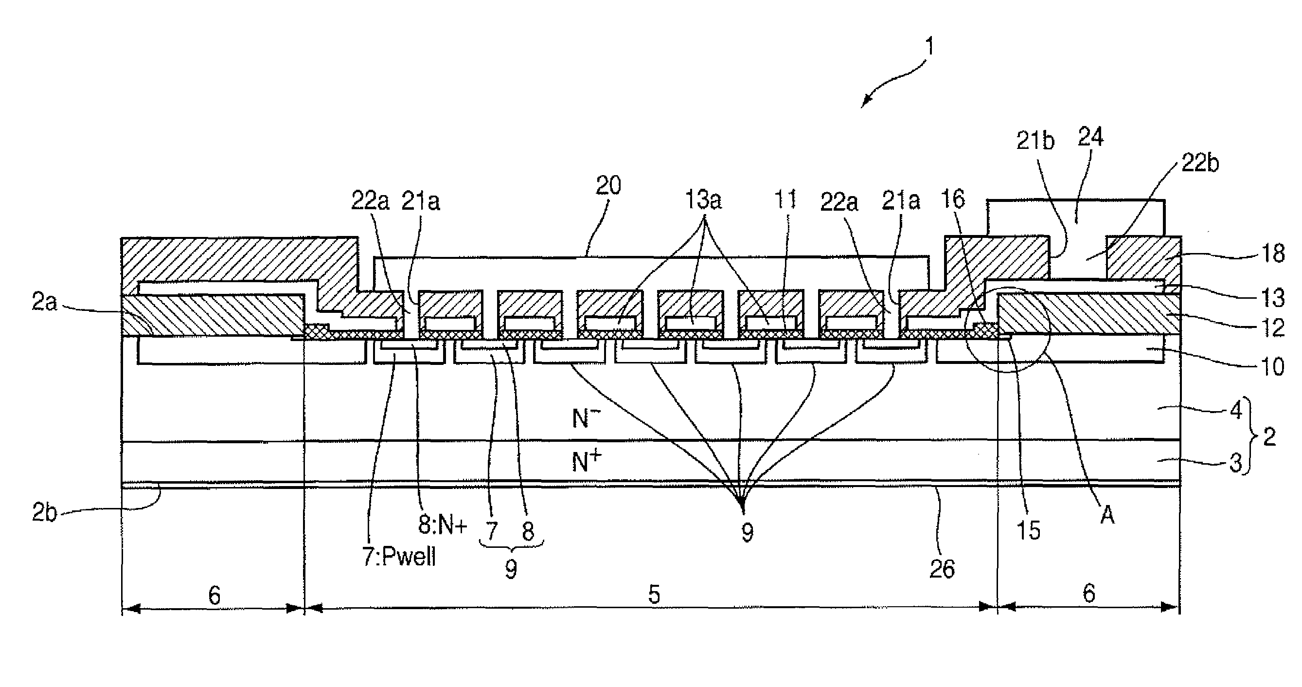
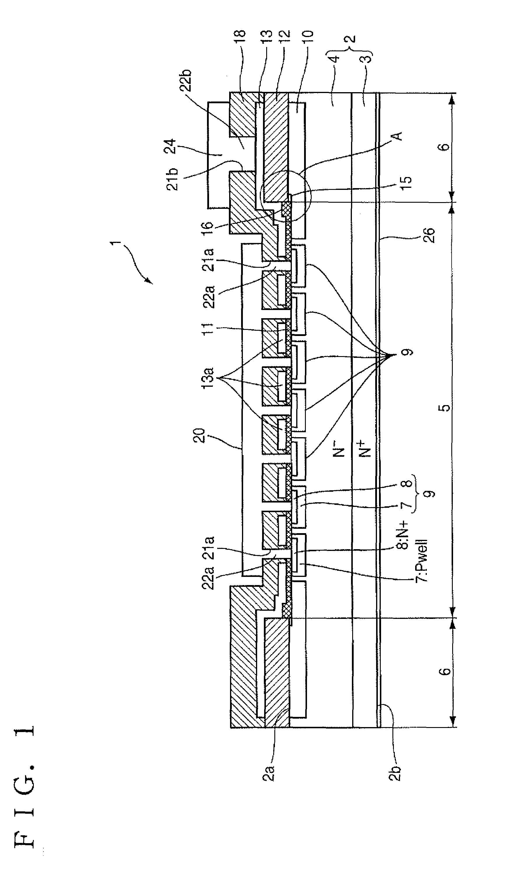
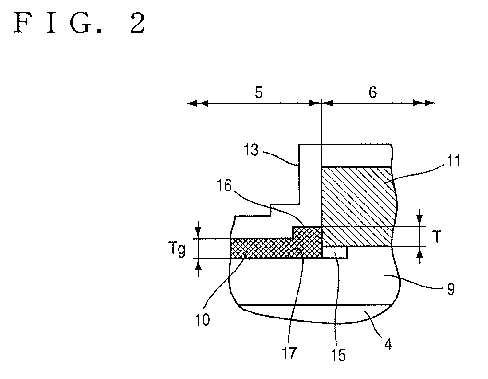
[0027]FIG. 1 is an explanatory view showing a section of a vertical nMOS transistor according to a first embodiment, FIG. 2 is an enlarged view illustrating a portion A shown in FIG. 1, and FIGS. 3 and 4 are respectively explanatory views showing a method for manufacturing the vertical nMOS transistor according to the first embodiment.

[0028]Reference numeral 1 indicates a vertical nMOS transistor (hereinafter called simply “nMOS”) used as a silicon carbide semiconductor device.

[0029]Reference numeral 2 indicates a silicon carbide substrate, which is a substrate having a crystal polymorph or polymorphism of 4H, in which silicon carbide is epitaxially grown on an N+ semiconductor substrate 3 made up of single-crystal silicon carbide, in which an N-type conductive impurity (hereinafter called “N-type impurity”) such as phosphorus (P), nitrogen (N) or the like used as a first conductivity type impurity is diffused in a relatively high concentration, thereby to form an N− semiconductor l...

second preferred embodiment

[0060]FIG. 5 is an explanatory view showing a partial section of a vertical nMOS transistor according to a second embodiment, FIG. 6 is an enlarged view illustrating a portion B shown in FIG. 5, and FIGS. 7 and 8 are respectively explanatory views showing a method for manufacturing the vertical nMOS transistor according to the second embodiment.

[0061]Incidentally, the same reference numerals are attached to portions or components similar to those in the first embodiment, and their description will therefore be omitted.

[0062]As shown in FIGS. 5 and 6, an amorphous layer 41 according to the present embodiment is formed with a thickness approximately equivalent to a thickness Tg (50 nm in the present embodiment) of a gate oxide film 11 by depositing amorphous silicon onto a frame-shaped area set in a manner similar to the first embodiments on a front surface 2a of an outer peripheral P-well layer 10 formed in an N− semiconductor layer 4 by using a thermal CVD method (refer to FIG. 7 (P...


PUM


Abstract

The present invention provides a silicon carbide semiconductor device comprising a semiconductor substrate comprising silicon carbide, which contains a first conductivity type impurity diffused therein in a high concentration, a semiconductor layer formed over the semiconductor substrate and containing the first conductivity type impurity diffused therein in a low concentration, a plurality of well regions formed on a front surface side of a cell forming area set to the semiconductor layer and in which a second conductivity type impurity corresponding to a type opposite to the first conductivity type impurity is diffused, source layers formed on the front surface side lying within the well regions and each containing the first conductivity type impurity diffused therein in a high concentration, an outer peripheral insulating film thick in thickness, which is formed over the semiconductor layer in an outer peripheral area that surrounds the cell forming area, a gate oxide film formed over the front surface of the semiconductor layer in the cell forming area, and a gate electrode layer formed so as to extend from above the gate oxide film to above the outer peripheral insulating film, wherein each of steplike portions adjacent to the outer peripheral insulating film and thicker than the gate oxide film in thickness is provided at an edge portion of the gate oxide film.

Description

BACKGROUND OF THE INVENTION[0001]The present invention relates to a silicon carbide semiconductor device such as a vertical power MOSFET designed for bulk power, formed in a silicon carbide substrate, and a manufacturing method thereof.[0002]A silicon carbide semiconductor device using a silicon carbide (SiC) crystal has a feature that it is excellent in electrical withstand-voltage characteristic and resists operations at high temperatures as compared with a normal semiconductor device using a silicon (Si) crystal.[0003]This is because as a result that the interatomic interval becomes shorter since the carbon (C) atom is contained, stronger interatomic bonding is obtained and the bandgap becomes larger than double, so that the withstand voltage characteristic is enhanced up to an electric field of more than double and the semiconductor characteristic is kept up to high temperatures.[0004]A MOSFET (Metal Oxide Semiconductor Field Effect Transistor) used as a conventional vertical si...

Claims


Application Information

Patent Timeline
IPC IPC(8): H01L23/373H01L21/8236H01L21/336H01L29/12H01L29/78
CPCH01L21/0465H01L21/8213H01L29/1608H01L29/66068H01L2924/0002H01L2924/00H01L29/7811
Inventor YOSHIE, TORU
Owner LAPIS SEMICON CO LTD
Why Eureka
Try Eureka