Photoelectric conversion element and solid-state imaging device

a technology of conversion element and photoelectric element, which is applied in the direction of thermoelectric devices, group 3/13 element organic compounds, methine/polymethine dyes, etc., can solve the problems of large device or apparatus size, poor light utilization efficiency, and increased cost, and achieve high photoelectric conversion efficiency, low noise, and good vapor deposition property

Inactive Publication Date: 2008-09-25
FUJIFILM CORP
View PDF11 Cites 94 Cited by
  • Summary
  • Abstract
  • Description
  • Claims
  • Application Information

AI Technical Summary

Benefits of technology

[0059]According to the second invention, a photoelectric conversion element containing a squarylium-based coloring matter and ensuring high photoelectric conversion efficiency and low noise as well as good vapor deposition property can be provided. Also, a photoelectric conversion element most suitable for a solid-state imaging device capable of simultaneously performing the photographing of a visible image based on visible light reflected from a photographic subject structure and the photographing of an infrared image based on infrared light can be provided.

Problems solved by technology

According to such a method, an image of visible light and an image of infrared light may be obtained at the same time, but these methods have problems, for example, that the size of the device or apparatus becomes large and the cost rises; the image is not sampled at the same point and the synthesis, processing and the like of image information are difficult; or the color filter transmits only light at a limited wavelength and the non-transmitted light is not utilized, giving rise to bad light utilization efficiency.
The system of stacking a photoelectric conversion part for detecting infrared light and a photoelectric conversion part for detecting visible light in the vertical direction is disadvantageous not only in that the absorption ranges are overlapped in respective portions in the depth direction of the silicone substrate and the color separation is originally poor due to bad spectral characteristics, but also in that when using Si, although a photoelectric conversion part for detecting infrared light must be further provided as the lowermost layer of the silicon substrate in the sensor of U.S. Pat. No. 5,965,875, infrared light is absorbed in the upper layer to reduce the infrared light reaching the lowermost layer in the silicon substrate and the sensitivity decreases.
However, in JP-A-63-186251, an upper Al electrode is used, which is insufficient in the transparency to visible light, and the contents disclosed therein are inadequate for imaging by visible light and infrared light.
In the electrophotographic technology, it is known that titanyl phthalocyanine and the like are widely used as an organic material sensitive to infrared light, but such a material has large absorption at a wavelength around 600 nm and is insufficient in the transparency to visible light.
Furthermore, the image-forming system using the existing structure and electric charging for the electrophotographic device is unsuited for a small imaging system without a light source, such as digital still camera, and can be hardly applied to a system of simultaneously taking the images of visible light and infrared light.
However, according to the studies by the present inventors, this material has a drawback that the current at the dark time (dark current) giving rise to a noise generally tends to become large in an imaging device and a high S / N can be hardly obtained.
However, when the present inventors studied on the photoelectric conversion performance of such a material, the photoelectric conversion performance was conspicuously low.
In this way, when the vapor deposition property is enhanced by providing a substituent working out to a steric hindrance, it is presumed that the signal electric charge transport property tends to deteriorate due to low intermolecular interaction.

Method used


Image

  • Photoelectric conversion element and solid-state imaging device
  • Photoelectric conversion element and solid-state imaging device
  • Photoelectric conversion element and solid-state imaging device

Examples


first embodiment

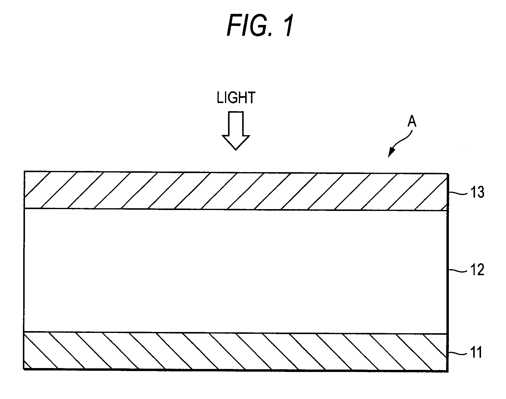
[0073]FIG. 1 is a cross-sectional schematic view roughly showing the construction of the photoelectric conversion element in the first embodiment of the present invention.

[0074]The photoelectric conversion element shown in FIG. 1 comprises at least a photoelectric conversion part A containing a lower electrode 11, an upper electrode 13 facing the lower electrode 11, and a photoelectric conversion film 12 provided between the lower electrode 11 and the upper electrode 13. The photoelectric conversion element shown in FIG. 1 is used by making light incident from the upper side of the upper electrode 13.

[0075]The upper electrode 13 is a transparent electrode composed of an electrically conductive material transparent to light (visible light and infrared light) in the combined range of a visible region and an infrared region (the range at a wavelength of 400 nm or more). The expression “transparent to light at a certain wavelength” as used in the present invention means that 70% or more...

second embodiment

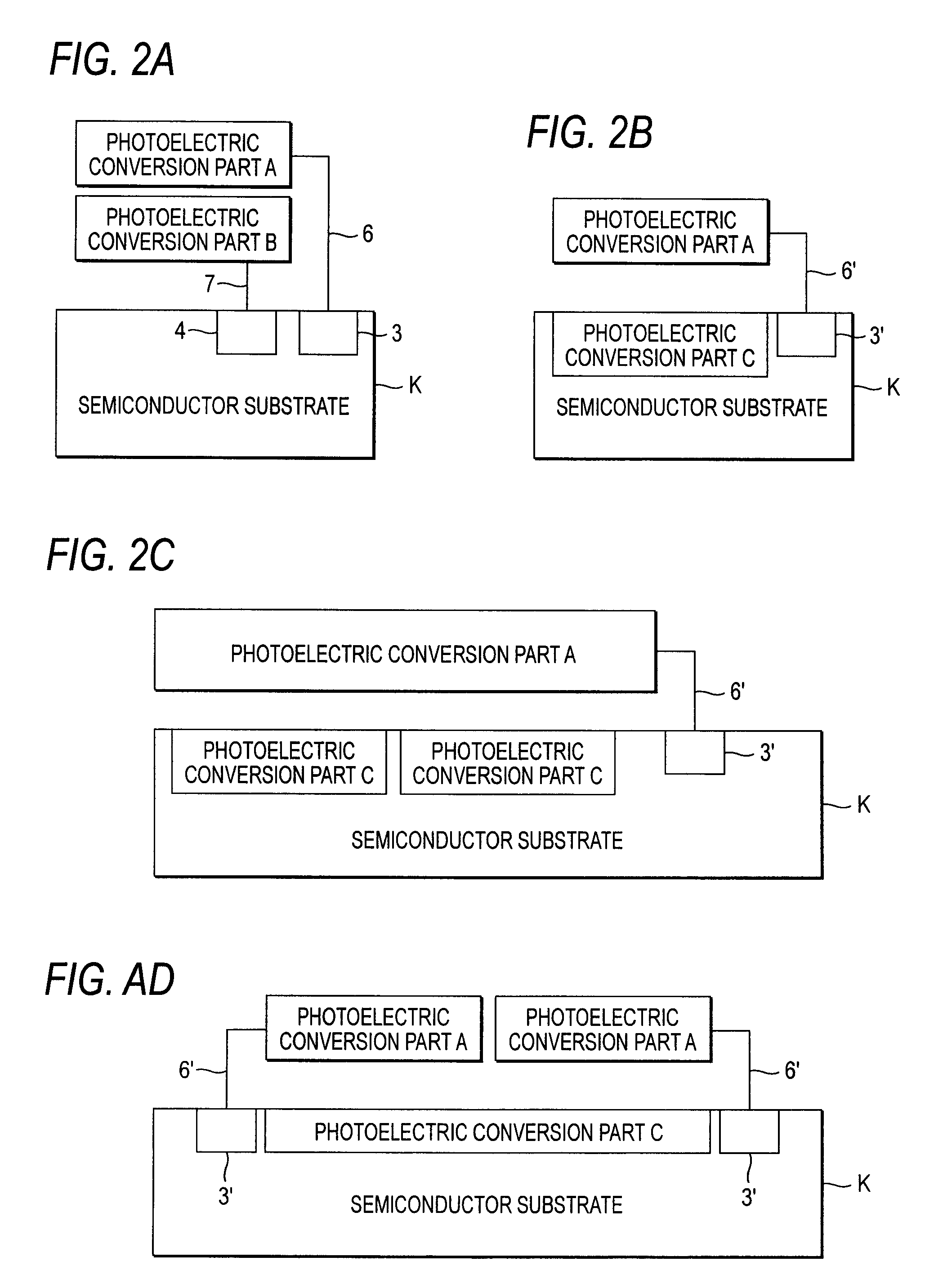
[0114]FIGS. 2A to 2D are cross-sectional schematic views roughly showing the construction of the photoelectric conversion element in the second embodiment of the present invention.

[0115]The photoelectric conversion element shown in FIG. 2A comprises a semiconductor substrate K such as silicon, a visible light photoelectric conversion part B stacked on the upper side of the semiconductor substrate K, and the photoelectric conversion part A shown in FIG. 1 stacked on the upper side of the visible light photoelectric conversion part B.

[0116]The visible light photoelectric conversion part B has almost the same construction as the photoelectric conversion part A and as for the organic photoelectric conversion material constituting the photoelectric conversion film 12 of the photoelectric conversion part A, a material having an absorption peak in the visible region of an absorption spectrum in the combined range of a visible region and an infrared region (the range at a wavelength of 400 ...

third embodiment

[0166]In this embodiment, a construction of realizing a solid-state imaging device by using the photoelectric conversion element having the construction shown in FIG. 2B is described.

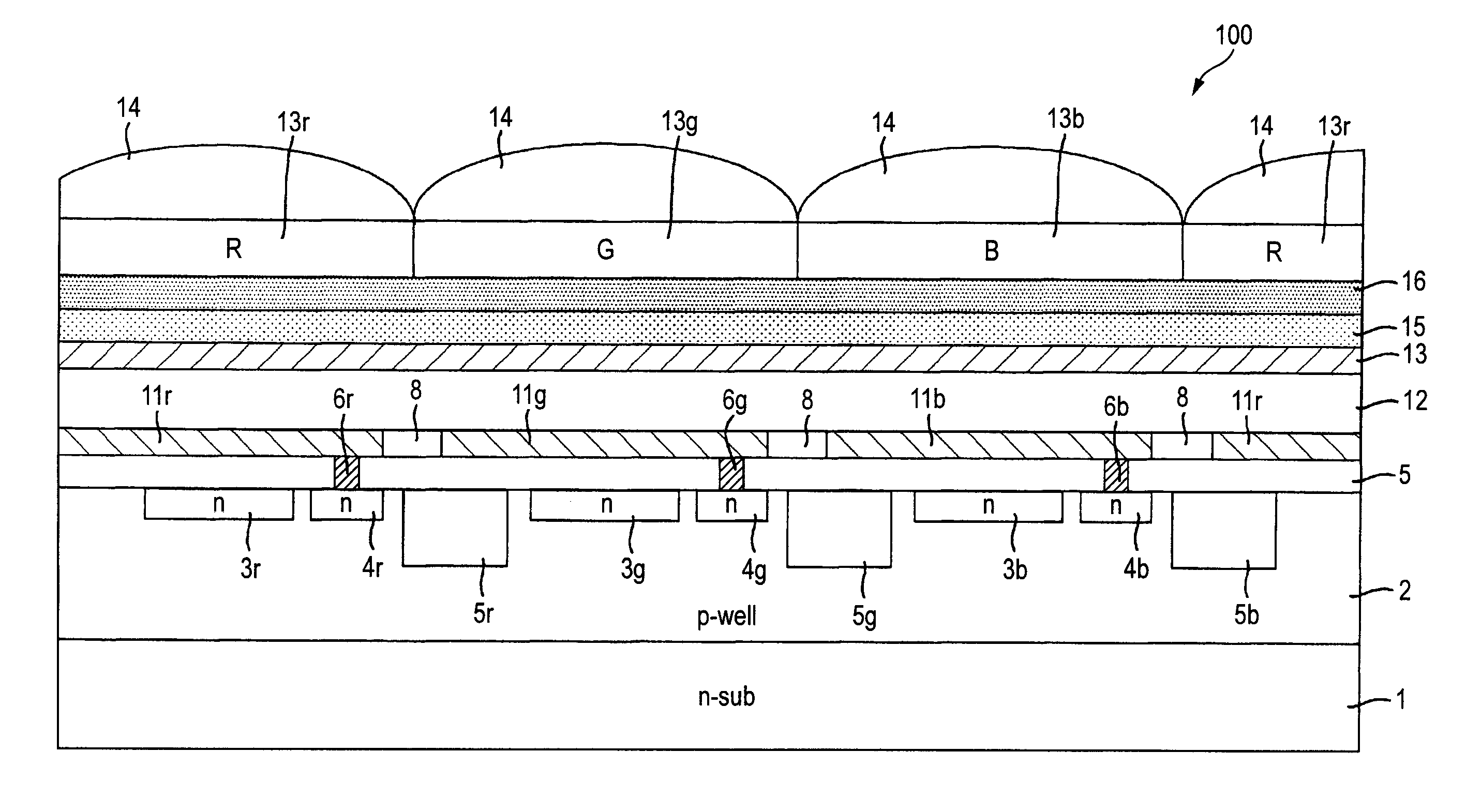
[0167]FIG. 4 is a partial surface schematic view of the imaging device for explaining the embodiment of the present invention, and FIG. 5 is a cross-sectional schematic view cut along the A-A line of the imaging device shown in FIG. 4. In FIG. 4, illustration of a microlens 14 is omitted. Also, in FIG. 5, the same constituents as those in FIG. 1 are indicated by the same numerical references.

[0168]A p-well layer 2 is formed on an n-type silicon substrate 1. In the following, the n-type silicon substrate 1 and the p-well layer 2 are collectively referred to as a semiconductor substrate. In the row direction and the column direction crossing the row direction at right angles on the same plane above the semiconductor substrate, three kinds of color filters, that is, a color filter 13r mainly transmitting R...


PUM

PropertyMeasurementUnit
transmittanceaaaaaaaaaa
decomposition temperatureaaaaaaaaaa

Abstract

A photoelectric conversion element comprises a first photoelectric conversion part, the first photoelectric conversion part comprising: a pair of electrodes; and a photoelectric conversion film between the pair of electrodes, wherein the photoelectric conversion film comprises an organic photoelectric conversion material having an absorption peak in an infrared region of an absorption spectrum within a combined range of a visible region and the infrared region and generating an electric charge according to light absorbed, and the first photoelectric conversion part as a whole transmits 50% or more of light in the visible region.

Description

BACKGROUND OF THE INVENTION[0001]1. Field of the Invention[0002]The present invention relates to a photoelectric conversion element comprising a photoelectric conversion part containing a pair of electrodes and a photoelectric conversion film provided between the pair of electrodes.[0003]The present invention relates to a photoelectric conversion element comprising a photoelectric conversion part containing a pair of electrodes and an infrared organic photoelectric conversion film provided between the pair of electrodes.[0004]2. Description of the Related Art[0005]The related-art visible light sensors in general are produced by forming a photoelectric conversion element through formation of PN junction in a semiconductor such as Si. As for the solid-state imaging device, there is widely known a flat-type image-receiving device where photoelectric conversion elements are two-dimensionally arrayed in a semiconductor and a signal generated resulting from photoelectric conversion is rea...

Claims


Application Information

Patent Timeline
Patent Type & Authority Applications(United States)
IPC IPC(8): H01L31/04C07D207/33H01L51/42
CPCC09B23/0066Y02E10/549H01L27/14621H01L27/14627H01L27/14632H01L27/14645H01L27/14687H01L27/14689H01L51/0062H01L51/0072H01L51/0078H01L51/4206H01L2251/308H01L51/4213H01L51/447H01L27/307C09B57/007H10K39/32H10K85/649H10K85/311H10K85/6572H10K30/10H10K30/451H10K30/87H10K2102/103
Inventor MITSUI, TETSUROKITAMURA, TETSUNOMURA, KIMIATSUHARADA, TORU
Owner FUJIFILM CORP
Why Eureka
Try Eureka