
Semiconductor memory device and manufacturing process therefore

a memory device and semiconductor technology, applied in the direction of semiconductor devices, electrical devices, transistors, etc., can solve the problems of increasing consumption current, increasing the difficulty of capacitor processing, and increasing the difficulty of capacitor removal, so as to facilitate the removal of a layer using cmp and stable circuit operation, the effect of high integration

Inactive Publication Date: 2008-09-25
ELPIDA MEMORY INC
View PDF2 Cites 6 Cited by
  • Summary
  • Abstract
  • Description
  • Claims
  • Application Information

AI Technical Summary

Benefits of technology

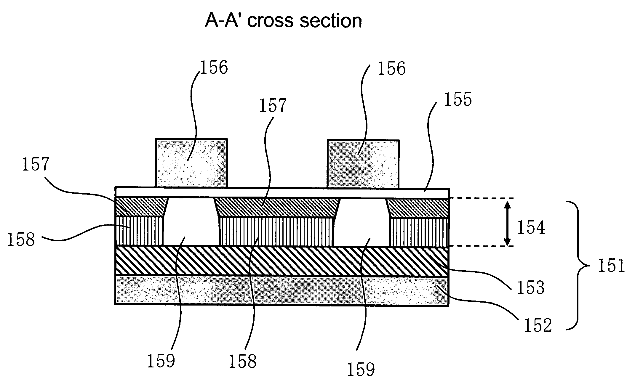
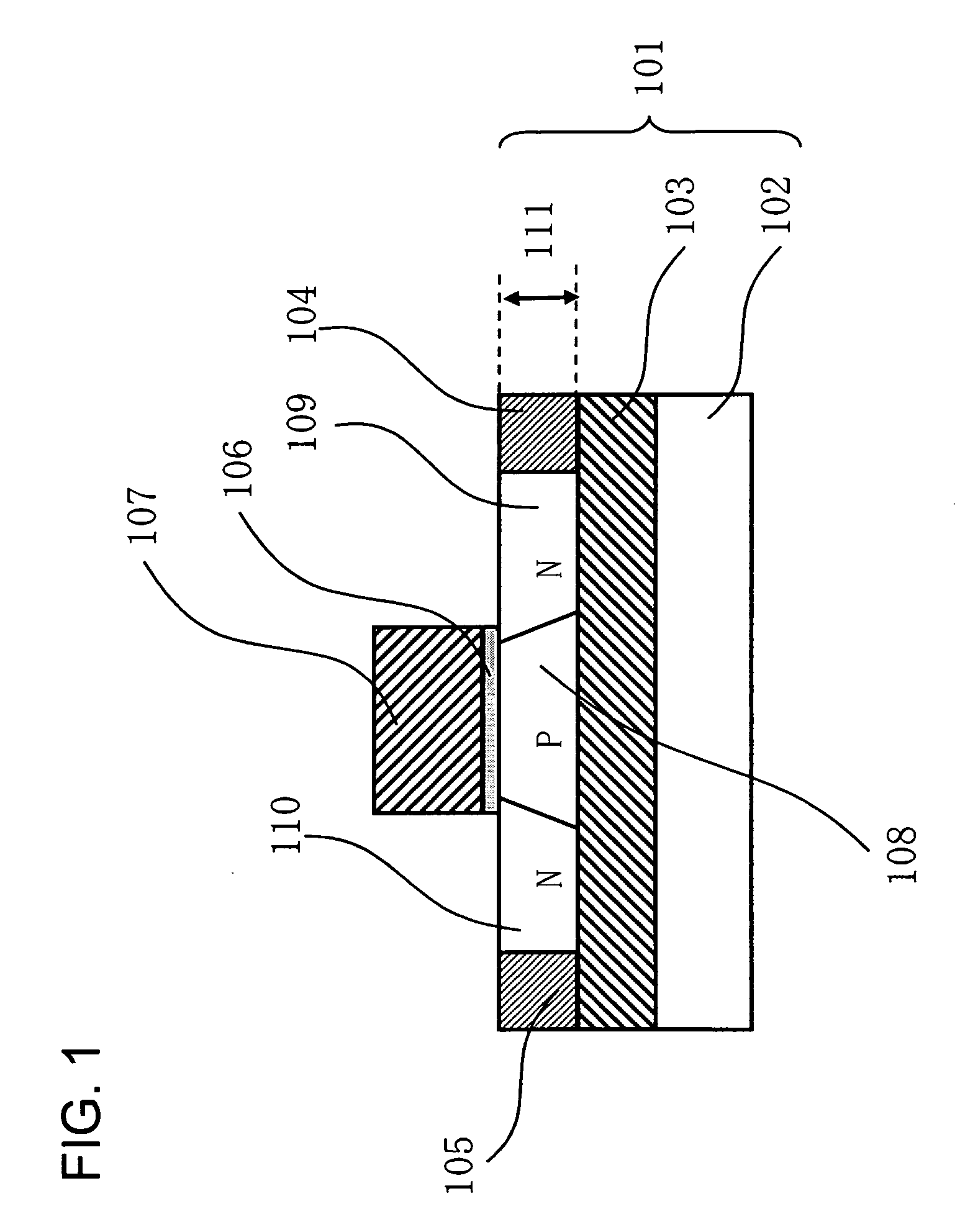
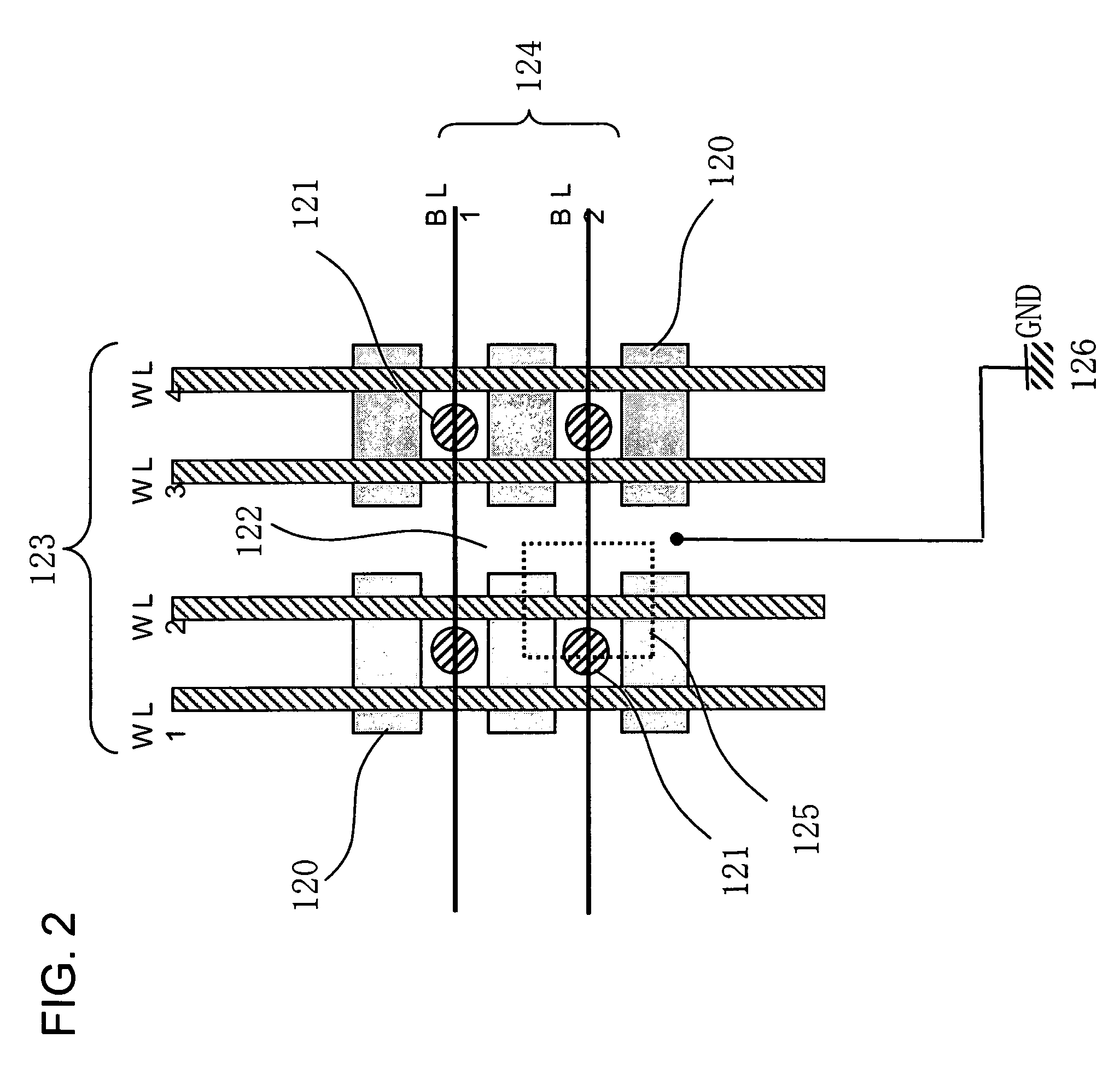
[0064]A semiconductor memory device of the present invention has a structure where an STI for isolation (isolation region A) in a memory cell region (first region) and a diffusion layer for a source region A / a drain region A in an MOS type transistor A extend from the surface of a semiconductor layer within an SOI type substrate to an insulating layer in a thickness direction. Thus, a body region (a region where a channel is to be formed) in a transistor in the memory cell region is in a floating state, allowing for capacitorless information storage utilizing hole accumulation effect.
[0065]On the other hand, a peripheral circuit region (second region) other than the memory cell region has a structure where both STI for isolation (isolation region B) and diffusion layer for a source region B / a drain region B in an MOS type transistor B extend from the surface of a semiconductor layer within the SOI type substrate to a depth not reaching the insulating layer in a thickness direction. In such a structure, the transistor in the peripheral circuit region can have fixed potentials of a body region and a well region, resulting in stable circuit operation without variation of a transistor threshold voltage.
[0066]In a semiconductor memory device of the present invention, while in the memory cell region and the peripheral circuit region an STI for isolation and an MOS type transistor have the above structure, the silicon layer in the surface of the SOI type substrate has an equal thickness in both the memory cell region and the periphery circuit region. Thus, the surface of the SOI type substrate is so flat that processings such as patterning using a photoresist film and removing a layer using CMP can be facilitated. It, therefore, allows a high-performance and highly integrated capacitorless DRAM to be easily formed.

Problems solved by technology

As a design rule has been increasingly size-reduced for achieving highly integrated DRAM, processing of, for example, a capacitor has become more difficult.
However, this floating structure becomes problematical for regions other than a memory cell (for example, a sense amplification circuit, a peripheral circuitry for input / output and a protection circuit for input / output).
Thus, circuit operation is so unstable that desired functions cannot be fulfilled or an operation current becomes larger, leading to increase in a consumption current.
However, it may cause another problem in terms of size reduction as described below.
As a result, a variety of problems as described below are caused during production, making it considerably difficult to produce a fine device with a higher integration degree.
For example, when trying to form a buried insulating film in an STI for isolation by CMP (Chemical Mechanical Polishing), polishing cannot be uniformly performed due to a difference in a surface height between these regions and, therefore, a desired shape cannot be obtained.
Furthermore, when a pattern is formed using a photolithography film, focus deviation occurs between regions having different surface heights during exposure, so that a pattern cannot be formed precisely in accordance with the mask shape.
Such manufacturing problems due to a height difference in substrate surface regions become more significant, as size reduction proceeds and an allowance in, for example, a dimension or film thickness in a manufacturing process becomes narrower.
Therefore, it is difficult to promote size reduction.

Method used


Image

  • Semiconductor memory device and manufacturing process therefore
  • Semiconductor memory device and manufacturing process therefore
  • Semiconductor memory device and manufacturing process therefore

Examples


example 1

[0179]There will be described a process for manufacturing Example 1 with reference to the drawings.

[0180]First, before describing all the steps in the manufacturing process for a semiconductor memory device of this example, there will be described a process for forming isolation regions having different depths (when using process (a) as the step of forming the isolation region A and the isolation region B).

[0181]FIGS. 8 to 13 are cross-sectional views of individual manufacturing steps, showing a process for forming isolation regions having different depths in the same semiconductor chip. In FIG. 8, 201 is an SOI type substrate consisting of three layers, that is, a lowermost silicon substrate (semiconductor substrate) 202, a silicon oxide layer (SiO2) 203 as an insulating layer and an upper silicon layer (semiconductor layer) 204.

[0182]First, a silicon oxide film 205 and a silicon nitride film (Si3N4) 206 were formed on the upper silicon layer 204 of the SOI type substrate. Then, pa...

example 2

[0203]There will be described a second example of a manufacturing process for a semiconductor memory device with reference to the drawings. FIGS. 19 to 21 are cross-sectional views illustrating a process for forming two isolation regions having different depths in Example 2 (when using process (b) as the step of forming the isolation region A and the isolation region B). The components described for Example 1 are denoted by the same numbers.

[0204]As shown in FIG. 19, a silicon oxide film 205 and a silicon nitride film 206 were formed on an SOI type substrate 201 consisting of three layers: a lower silicon substrate (semiconductor substrate) 202, a silicon oxide layer (insulating layer) 203 and an upper silicon layer (semiconductor layer) 204. Then, patterning was conducted to form a trench (hole) 220 and a trench B 221 for an isolation region. Here, an etching depth of trench 220 in the silicon layer 204 is the same as that in trench 221, that is, an etching amount was adjusted such...

example 3

[0211]Next, Example 3 will be described with reference to the drawings. FIGS. 22 to 24 are cross-sectional views showing a process for forming two isolation regions having different depths in Example 3 (when using process (c) as the step of forming the isolation region A and the isolation region B). The components described in Example 2 are denoted by the same numbers.

[0212]First, to the step of FIG. 19 illustrated in Example 2, a trench A 220 and a trench B 221 for isolation region which had the same depth and did not reach the silicon oxide layer 203 were formed as described in Example 2.

[0213]Next, as shown in FIG. 22, only the trench B 221 for isolation formed in the region where a shallow isolation region B is to be formed was covered by the photoresist film 222. Then, a region C 225 from the bottom of the trench B 220 to the insulating layer in a thickness direction was ion-implanted with oxygen at a dose of 1×10¹⁵ to 1×10¹⁶ ions / cm2 and an implantation energy of 20 to 100 KeV...


PUM


Abstract

An objective of this invention is to solve the problem caused by a difference in a silicon layer film thickness between a memory cell region and a region other than the memory cell region.For solving the problem, while maintaining a structure where an MOS type transistor in a memory cell region is in a floating state and an MOS type transistor in the region other than the memory cell region is not in a floating state, a film thickness of semiconductor layers having a body regions is made equal in these MOS type transistors.

Description

[0001]This application is based upon and claims the benefit of priority from Japanese Patent Application No. 2007-058799, filed on Mar. 8, 2007, the disclosure of which is incorporated herein in its entirety by reference.BACKGROUND OF THE INVENTION[0002]1. Field of the Invention[0003]The present invention relates to a semiconductor memory device comprising a capacitorless DRAM in which one memory cell is made up of one transistor and comprising an SOI type substrate and a process for manufacturing a semiconductor memory device.[0004]2. Description of the Related ArtMemory Cell Manufactured Using a Related Floating-Body Type MOS Transistor[0005]In a related DRAM (Dynamic Random Access Memory), one memory cell is made up of a combination of one MOS transistor and one capacitor. As a design rule has been increasingly size-reduced for achieving highly integrated DRAM, processing of, for example, a capacitor has become more difficult. There has been, therefore, suggested a capacitorless ...

Claims


Application Information

Patent Timeline
Patent Type & Authority Applications(United States)
IPC IPC(8): H01L27/12H01L21/84
CPCH01L21/84H01L27/108H01L27/10802H01L29/78618H01L27/1203H01L29/7841H01L27/10894H10B12/20H10B12/00H10B12/09
Inventor OHARA, SHINJI
Owner ELPIDA MEMORY INC
Learn More