Information recording/reproducing device

a recording/reproducing device and information technology, applied in the field of information recording/reproducing devices with high, can solve the problems of insufficient realization of new information recording media using such new recording materials, and too large consumption, and achieve the effect of low power consumption and high thermal stability

Inactive Publication Date: 2008-10-02
KK TOSHIBA
View PDF1 Cites 30 Cited by
  • Summary
  • Abstract
  • Description
  • Claims
  • Application Information

AI Technical Summary

Benefits of technology

[0015]The present invention proposes a nonvolatile information recording / reproducing device with low power consumption and high thermal stability.
[0020]According to an example of the present invention, it is possible to realize a nonvolatile information recording / reproducing device with a low power consumption and a high thermal stability, by making cations easily diffusable and maintaining a host structure stably, while using a recording layer having a “Wolframite structure and / or similar one” or “Scheelite structure and / or similar one”.

Problems solved by technology

However, a new information recording medium using such new recording materials has not been realized, because the power consumption is too large and the thermal stability in each resistance state is too low (for instance, refer to S. Seo et al.

Method used


Image

  • Information recording/reproducing device
  • Information recording/reproducing device
  • Information recording/reproducing device

Examples


first example

[0204

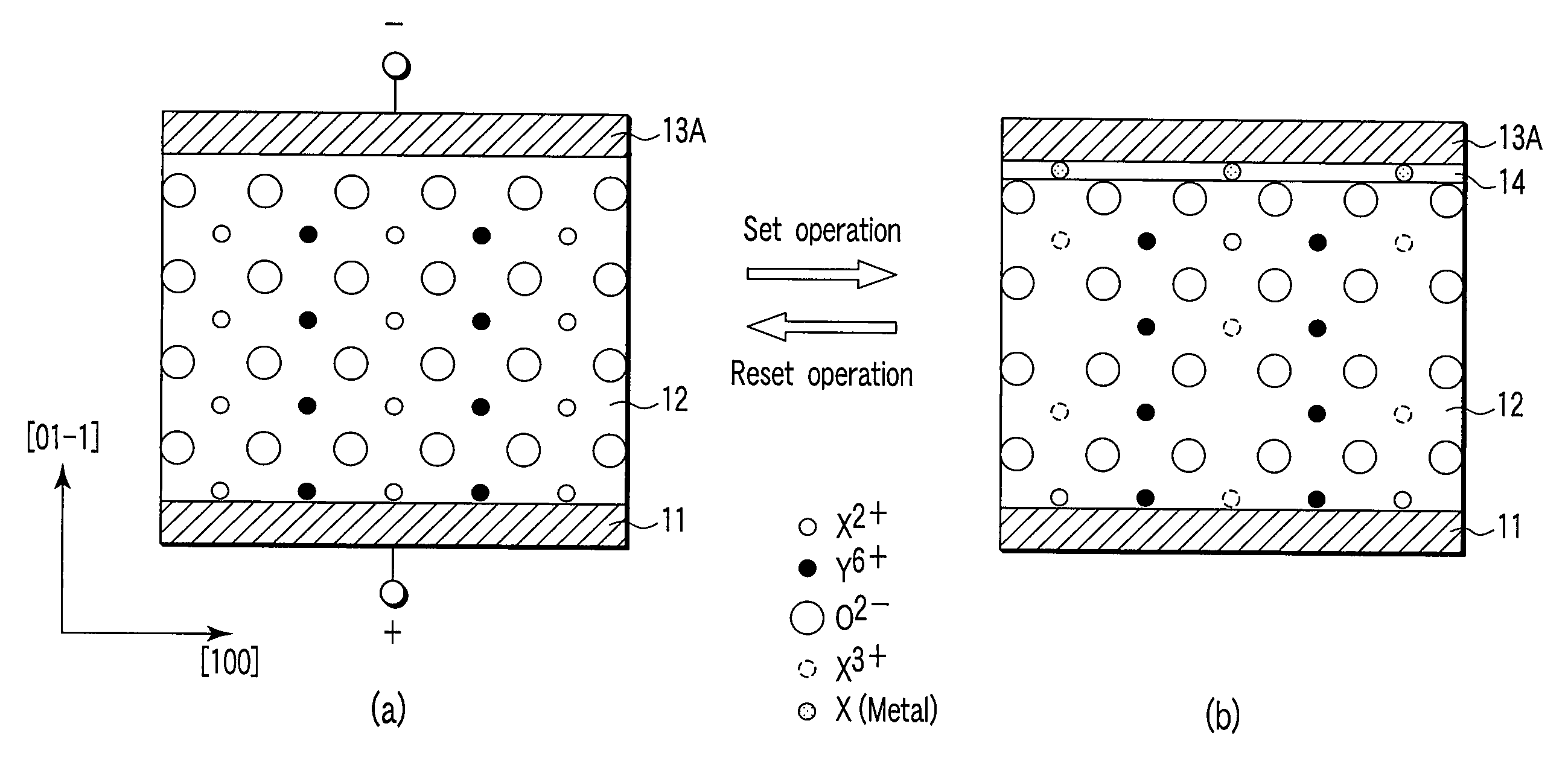
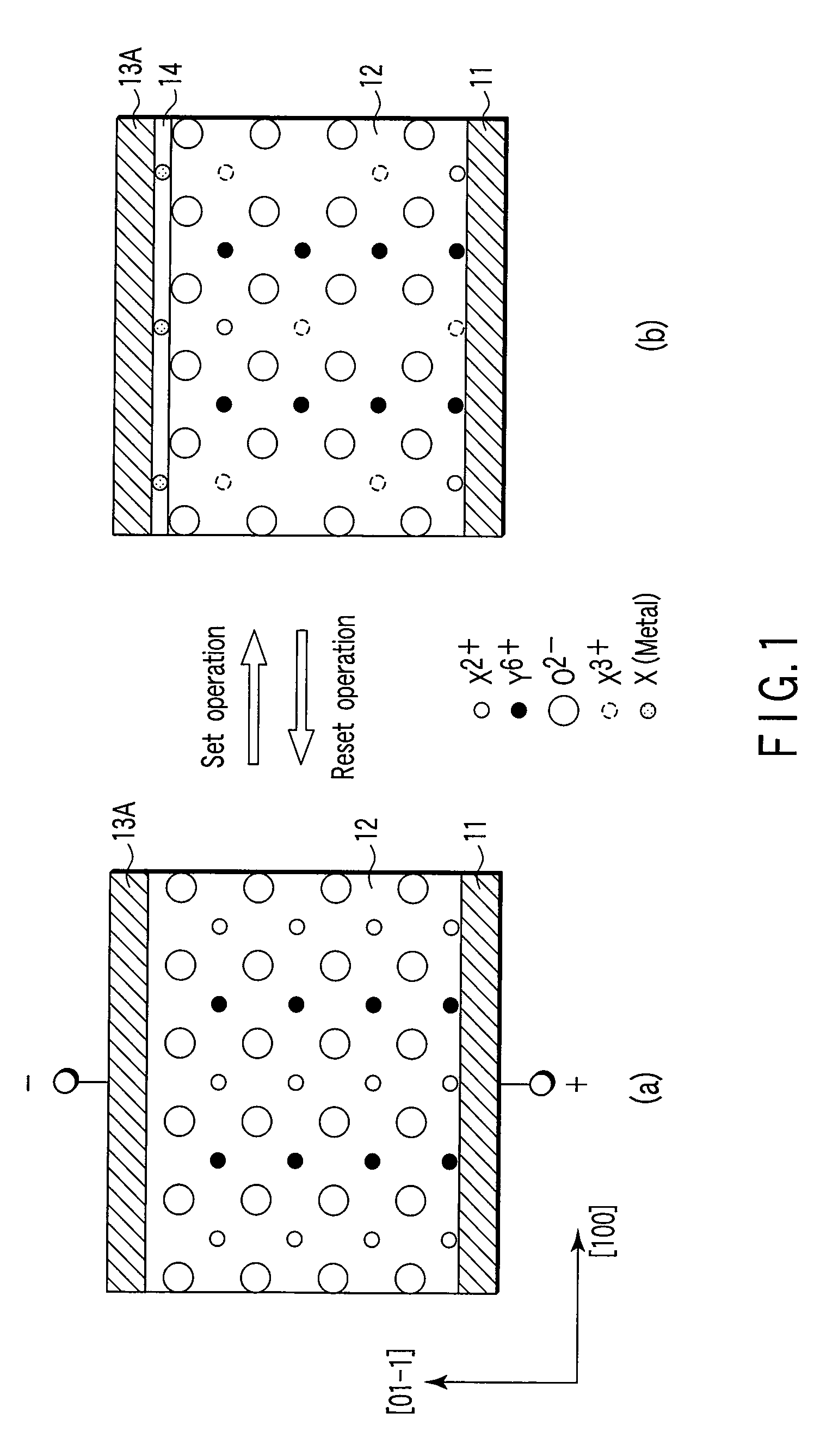
[0205]The first example is a case where the materials of FIG. 1 are used for the recording layer.

[0206]Firstly, as shown in FIG. 7, there is prepared a state where the electric potential of the probe 24 is relatively lower than the electric potential of the electrode layer 21. The probe 24 may be supplied with a negative electric potential, when the electrode layer 21 has a fixed electric potential, for instance, ground potential.

[0207]The current pulse is generated by emitting electrons toward the electrode layer 21 from the probe 24 while using, for instance, an electron generating source or hot electron source. Alternatively, it is also possible to bring the probe 24 into contact with the surface of the recording bit 27 to apply the voltage pulse.

[0208]At this time, for instance, in the recording bit 27 of the recording layer 22, part of X ions moves to the probe (cathode) 24 side, and the number of X ions inside the crystal relatively decreases in comparison to the number o...

second example

[0218

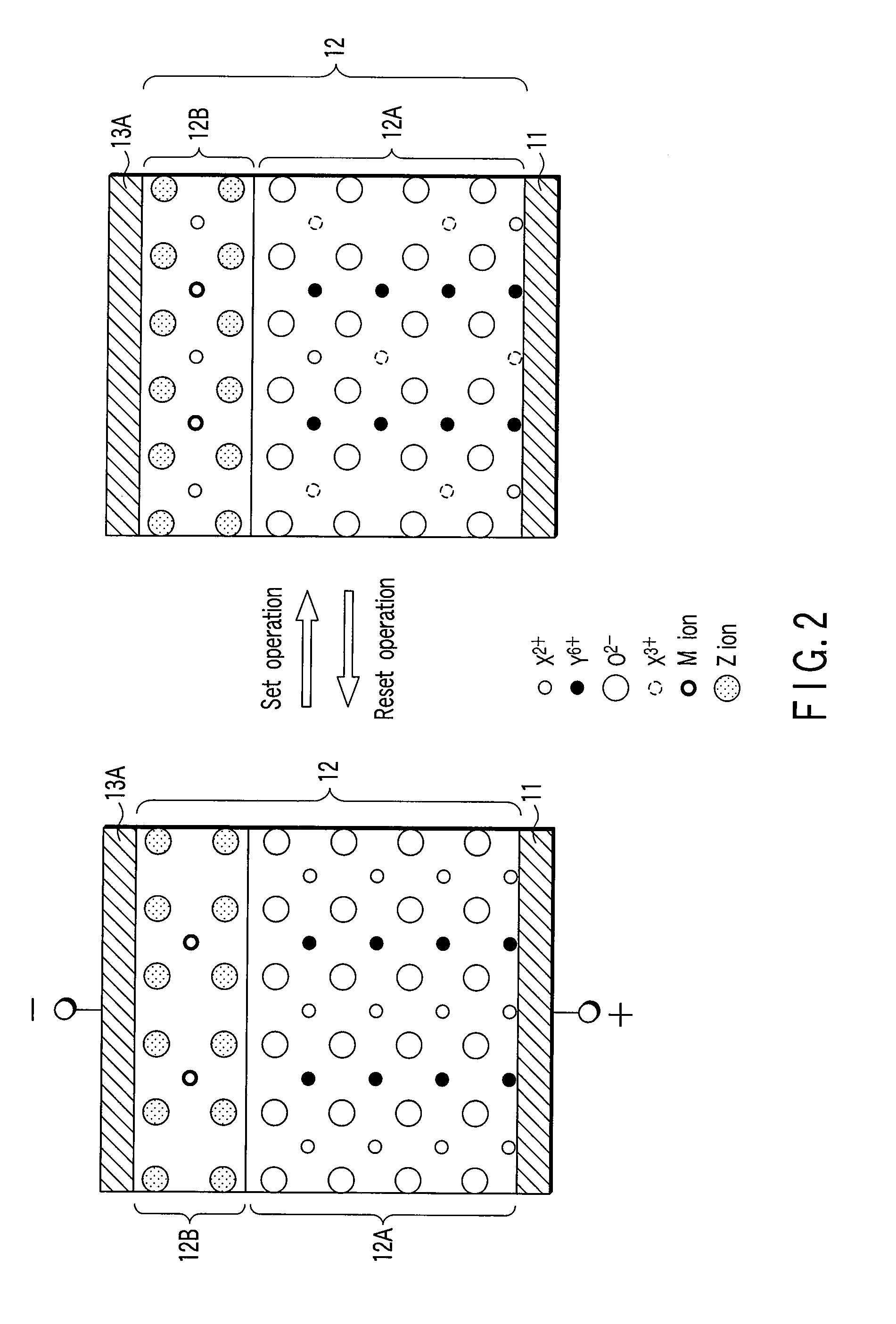
[0219]The second example shows a case where the materials of FIG. 2 are used for the recording layer.

[0220]Firstly, as shown in FIG. 9, there is prepared a state where the electric potential of the probe 24 is relatively lower than the electric potential of the electrode layer 21. It is only necessary to supply a negative potential to the probe 24 when the electrode layer 21 has a fixed electric potential, for instance, ground potential.

[0221]At this time, part of X ions inside the first chemical compound (anode side) 12A of the recording layer 22 is accommodated in the vacant site of the second chemical compound (cathode side) 12B while moving inside the crystal. With this, the valence of X ions inside the first chemical compound 12A increases, while the valence of M ions inside the second chemical compound 12B decreases. As a result, conductive carriers are generated inside the crystal of the first and second chemical compounds 12A, 12B, and then both come to have the electri...

experiment example

[0230]C. Experiment Example

[0231]The recording medium having the structure shown in FIG. 7 is used as a sample, and evaluation may be performed by using a pair of acicular probes whose diameter of a leading edge is 10 nm or less.

[0232]The electrode layer 21 is, for instance, a Pt film formed on a semiconductor substrate. In order to increase adhesion properties between the semiconductor substrate and a lower electrode, Ti of about 5 nm may be used as an adhesion layer. The recording layer 22 can be obtained by performing RF magnetron sputtering on a disk in a mixed gas of argon and oxygen while maintaining the temperature of the disk at a high temperature of about 600° C., by using a target in which components are adjusted so as to have the desired composition. Further, as the protection layer, for instance, diamond-like carbon may be formed by the CVD method. The film thickness of the respective layers can be designed so as to optimize a resistance ratio between the low resistance ...


PUM


Abstract

There is proposed a nonvolatile information recording / reproducing device with low power consumption and high thermal stability. The information recording / reproducing device according to an aspect of the present invention includes a recording layer, and mechanism for recording information by generating a phase change in the recording layer while applying a voltage to the recording layer. The recording layer is comprised one of a Wolframite structure and a Scheelite structure.

Description

CROSS REFERENCE TO RELATED APPLICATIONS[0001]This is a Continuation Application of PCT Application No. PCT / JP2007 / 061828, filed Jun. 12, 2007, which was published under PCT Article 21(2) in Japanese.[0002]This application is based upon and claims the benefit of priority from prior Japanese Patent Application No. 2007-094628, filed Mar. 30, 2007, the entire contents of which are incorporated herein by reference.BACKGROUND OF THE INVENTION[0003]1. Field of the Invention[0004]The present invention relates to an information recording / reproducing device with a high recording density.[0005]2. Description of the Related Art[0006]In recent years, compact portable devices have been widely used worldwide and, at the same time, a demand for a small-sized and large-capacity nonvolatile memory has been expanding rapidly along with the extensive progress of a high-speed information transmission network. Among them, particularly a NAND type flash memory and a small-sized HDD (hard disk drive) have...

Claims


Application Information

Patent Timeline
Patent Type & Authority Applications(United States)
IPC IPC(8): G11C11/00
CPCB82Y10/00G11B9/04G11B9/1436G11B9/1481G11B9/149G11C13/00G11C13/0004G11C13/0007G11C2213/31G11C2213/32G11C2213/51G11C2213/52G11C2213/56G11C2213/71G11C2213/72G11C2213/79H01L27/115H01L27/11517H01L27/2409H01L27/2481H01L45/1233H01L45/1253H01L45/126H01L45/147H01L45/1625H01L45/085H10B63/84H10B63/20H10N70/245H10N70/8413H10N70/841H10N70/8836H10N70/026H10N70/826H10B41/00H10B69/00
Inventor TSUKAMOTO, TAKAYUKIKUBO, KOHICHIKAMATA, CHIKAYOSHIHIRAI, TAKAHIROAOKI, SHINYAHIRAOKA, TOSHIRO
Owner KK TOSHIBA
Why Eureka
Try Eureka