Method of preparing highly thermally conductive circuit substrate

a technology of circuit substrate and thermally conductive substrate, which is applied in the direction of resistive material coating, chemical vapor deposition coating, solid-state device coating, etc., can solve the problems of defective thermally conductive substrate, low peel strength, and sub-substrates that are also subject to peeling, so as to improve the adhesion of electrically conductive main layer, accelerate the process, and improve the structural strength

Inactive Publication Date: 2008-10-16
COSMOS VACUUM TECH CORP
View PDF10 Cites 0 Cited by
  • Summary
  • Abstract
  • Description
  • Claims
  • Application Information

AI Technical Summary

Benefits of technology

[0009]The primary objective of the present invention is to provide a method of preparing a highly thermally conductive circuit substrate, which accelerates the manufacturing process.
[0010]The secondary objective of the present invention is to provide a method of preparing a highly thermally conductive circuit substrate, which enhances the adhesion of the electrically conductive layer and thickens the same to enable preferable electrical conductivity.
[0012]The foregoing objectives of the present invention are attained by the method including the steps of preparing a metallic substrate, producing an insulated layer on a surface of the metallic substrate, producing an intermediate medium layer on a surface of the insulated layer, and producing an electrically conductive main layer on a surface of the intermediate medium layer by electrochemical technology. In light of these steps, the intermediate medium layer balances the physical property of the insulated layer and the electrically conductive main layer to enhance the adhesion of the electrically conductive main layer, such that the circuit substrate can have preferable structural strength. Furthermore, the present invention employs the electrochemical technology for post manufacturing process of the electrically conductive main layer to further accelerate the process. In addition, the present invention provides another step of producing the insulated layer to further increase the regularity of the crystal morphology of the insulated layer, thus having preferable thermal conductivity.

Problems solved by technology

The substrate is also subject to peeling, i.e. the peel strength is low.
However, the thickness of the above-mentioned metallic film 3 made by the vacuum coating is 9 μm at most and if it is more than 9 μm, the metal film 3 may peel off, such that the above-mentioned thermally conductive substrate is defective in that the metallic film 3 is too thin to have preferable electrical conductivity.
Furthermore, the vacuum coating by which the electrically conductive film is made is slower in formation of the film to defectively take more working hours.
In other words, the vacuum coating that the electrically conductive film is made has drawbacks of imperfect electric conductivity and costing more working hours.
In light of the above, the conventional thermally conductive substrate is defective to cost more working hours and to have lower production efficiency as well as imperfect thermal conductivity.

Method used


Image

  • Method of preparing highly thermally conductive circuit substrate
  • Method of preparing highly thermally conductive circuit substrate
  • Method of preparing highly thermally conductive circuit substrate

Examples


Embodiment Construction

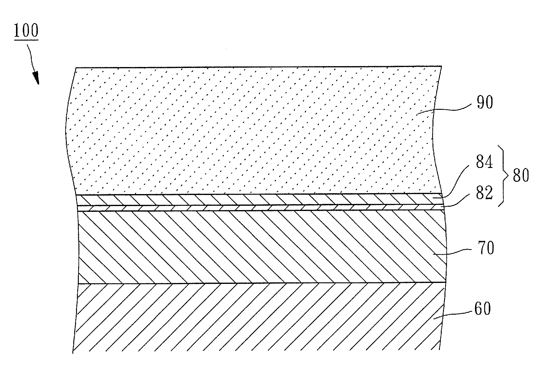
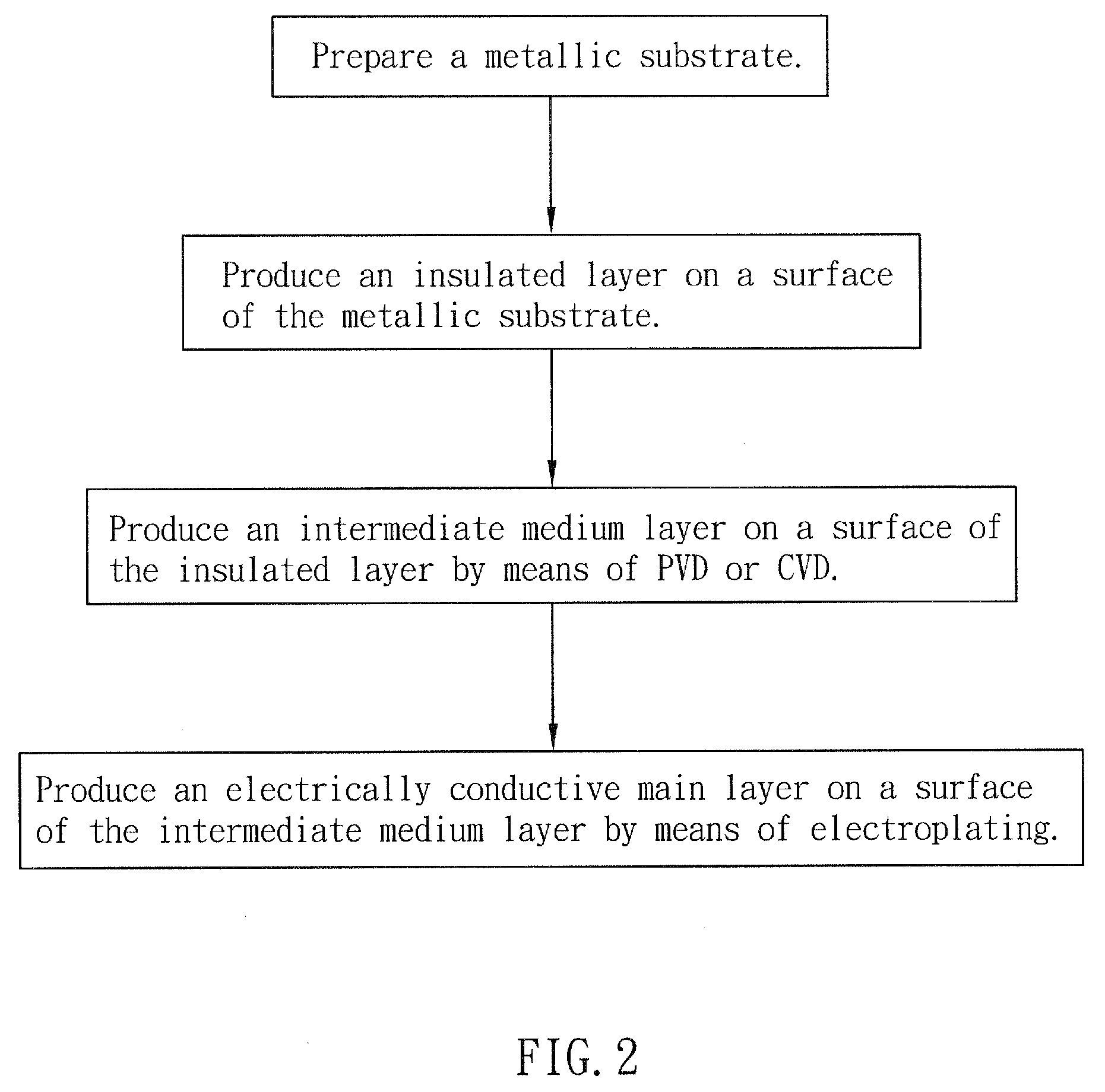
[0021]Referring to FIGS. 2-7, a method of preparing a highly thermally conductive circuit substrate according to a first preferred embodiment of the present invention includes the following steps.

[0022]A. Prepare a metallic substrate 10. The metallic substrate 10 is made of a material selected from a group consisting of aluminum, magnesium, titanium, and an alloy of them. In this embodiment, the metallic substrate 10 is made of aluminum.

[0023]B. Produce an insulated layer 20 on a surface of the metallic substrate 10. The insulated layer 20 is made of a compound of at least one of aforementioned metals. In this embodiment, the insulated layer 20 is made of an oxide of at least one of the aforementioned metals. The insulated layer 20 is aluminum trioxide formed on the surface of the metallic substrate 10 by means of general anodizing, such as MAO anodizing and plasma electrolytic oxidation (PEO). However, to enable preferable thermal conductivity of the insulated layer 20 of aluminum ...


PUM

PropertyMeasurementUnit
voltageaaaaaaaaaa
thicknessaaaaaaaaaa
thicknessaaaaaaaaaa

Abstract

A method of preparing a highly thermally conductive circuit substrate includes the steps of preparing a metallic substrate, producing an insulated layer on a surface of the metallic substrate, producing an intermediate medium layer on a surface of the insulated layer, and producing an electrically conductive main layer on a surface of the intermediate medium layer.

Description

BACKGROUND OF THE INVENTION[0001]1. Field of the Invention[0002]The present invention relates generally to surface treatment technology, and more particularly, to a method of preparing a highly thermally conductive circuit substrate.[0003]2. Description of the Related Art[0004]Referring to FIG. 1, Taiwan Patent Pre-grant No. 200520670 disclosed an integrated thermally conductive substrate and a method of preparing the same. The method includes the steps of preparing a metallic substrate 1, producing an insulated layer 2 made of aluminum trioxide on the metallic substrate 1 by means of micro arc oxidation (MAO) anodizing for thermal conduction, and disposing a metallic film 3, which is made of copper and has a predetermined design, on the insulated layer with a vacuum-coated film to define a plurality of metal wires and to produce an integrated thermally conductive substrate 4. This invention is for the purpose of integration, thermal conduction, and circuit layout in such a way that...

Claims


Application Information

Patent Timeline
Patent Type & Authority Applications(United States)
IPC IPC(8): C25D5/00B05D5/12C25D11/02
CPCC25D5/34C25D11/04H01L2924/0002H01L21/4871H01L23/142H01L23/3735H05K1/053H05K3/388H05K2203/0315C23C28/322C23C28/3225C23C28/345C23C28/3455C25D11/026H01L2924/00
Inventor HUANG, HSU-TANCHOU, CHUNG-LIN
Owner COSMOS VACUUM TECH CORP
Why Eureka
Try Eureka