Nonvolatile semiconductor memory device and manufacturing method thereof

a non-volatile, memory device technology, applied in semiconductor devices, transistors, instruments, etc., can solve the problems of increasing the capacitive coupling between floating gates, the inability to use current and future flash memory, and the reduction of the size of the memory cell, so as to reduce the pitch of the control gate (word line), the effect of reducing the threshold voltage shift of the memory cell and improving programming/erasing performan

Inactive Publication Date: 2008-10-23
SASAGO YOSHITAKA +1
View PDF3 Cites 7 Cited by
  • Summary
  • Abstract
  • Description
  • Claims
  • Application Information

AI Technical Summary

Benefits of technology

[0009]It is the general objective of the present invention to provide a technique for reducing the capacitance between adjoining floating gates, and for lowering the threshold voltage shift by interference between adjoining memory cells in a nonvolatile semiconductor memory device in which a reduction in the memory cell size has progressed since 90 nm generation.
[0015]In a nonvolatile semiconductor memory device, the threshold voltage shift of the memory cell caused by capacitive coupling between the adjoining floating gates becomes remarkable with decreasing the pitch of the control gate (word line). The threshold voltage shift of the memory cell can be reduced by decreasing the opposing area between the adjoining floating gates. Because of this, the threshold value level gap of each state of the memory cell can be made narrower, so that the programming / erasing performance can be improved. Moreover, it has the effect of preventing a read error by the above-mentioned threshold voltage shift of the memory cell, resulting in the reliability of the nonvolatile semiconductor memory device being improved.

Problems solved by technology

That is, it is impossible for it to be used in a current and future flash memory in which the floating gate and word line have to be fabricated in the minimum feature size.
Additionally, a new problem arises in the aforementioned non-patent documents 1 and 2 when the reduction in memory cell size progresses further.
That is, there is the problem that the capacitive coupling between the floating gates becomes larger, and the interference between the adjoining floating gates becomes larger because the gap between the adjoining floating gates becomes smaller.
Especially, in the case when a multilevel storage technique is used, it causes the performance and reliability to be decreased because it is necessary to make the threshold voltage gap of each level larger taking into consideration the threshold voltage shift.
Therefore, from the 90 nm generation on, a reduction in the bit cost using a multilevel storage technique and maintaining the programming / erasing speed have not been compatible.

Method used


Image

  • Nonvolatile semiconductor memory device and manufacturing method thereof
  • Nonvolatile semiconductor memory device and manufacturing method thereof
  • Nonvolatile semiconductor memory device and manufacturing method thereof

Examples


first embodiment

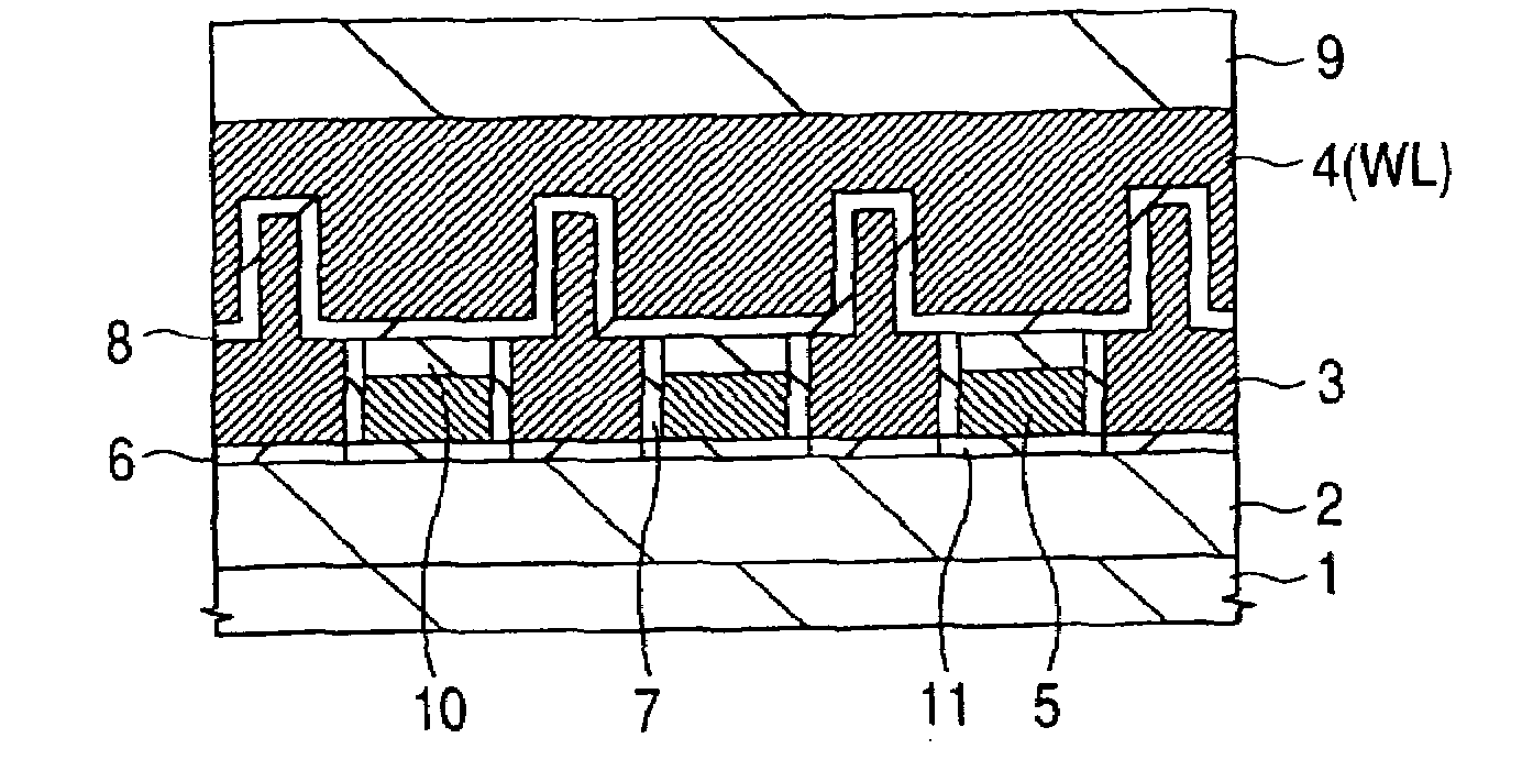
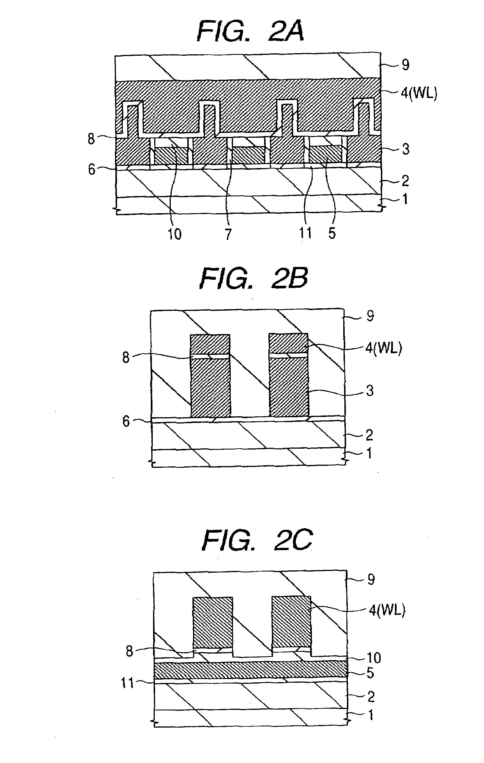
[0080]FIG. 1 is a main plane diagram schematically illustrating one example of a nonvolatile semiconductor memory device described in the first embodiment of the present invention. FIGS. 2A, 2B, and 2C are main cross-sectional views at the positions of line A-A′, line B-B′, and line C-C′ of FIG. 1, respectively. FIG. 3 is a schematic circuit diagram of a memory array illustrating the first embodiment of a nonvolatile semiconductor memory device of the present invention. A part of the material section is omitted to make the diagram easy to see.

[0081]The nonvolatile semiconductor memory device described in the first embodiment of the present invention comprises a so-called memory cell of a flash memory, wherein this memory cell comprises a well 2 formed on the main surface of the semiconductor substrate 1, the floating gate (first gate) 3, the control gate (second gate) 2, and the third gate 5.

[0082]The control gate 4 of each memory cell is connected along the line direction (X direct...

second embodiment

[0099]In the aforementioned first embodiment, the shape of the floating gate was made in an inverse T-shape by isotropically etching a part of the stripe-shaped polysilicon film, but it can be made in an inverse T-shape by forming the floating gate in two polysilicon layers.

[0100]FIGS. 13 to 16 are main cross-sections and main plane diagrams schematically illustrating one example of a nonvolatile semiconductor memory device described in the second embodiment of the present invention.

[0101]First, the same as the processes described in FIGS. 5A to 7A of the aforementioned first embodiment, the fourth insulator film 7 is formed along the side walls of the dummy silicon oxide film pattern 12 patterned in a stripe shape, the fifth insulator film 10, and the third gate 5. And then, the polysilicon film 3a which will become the first layer of the floating gate is deposited to completely fill the space of the stripe-shaped pattern. Next, the polysilicon film 3a is partially removed by etch ...

third embodiment

[0109]In the aforementioned second embodiment, the space for forming the polysilicon pattern of the second layer of the floating gate was fabricated by etching back the first layer of the floating gate. On the other hand, in the third embodiment, another example to fabricate a space will be described in which the polysilicon pattern of the second layer is formed

[0110]FIGS. 17 to 22 are main plane diagrams schematically illustrating one example of a nonvolatile semiconductor memory device described in the third embodiment of the present invention.

[0111]First, a p-well 2 is formed on the semiconductor substrate 1, and the gate insulator film 11 with a thickness of about 10 nm is formed on the well 2 by, for instance, a thermal oxidation method (FIG. 17A).

[0112]Next, a phosphorus-doped polysilicon film 5a which will become the third gate, and the silicon nitride film 10a which will become the fifth insulator film are deposited in order (FIG. 17B).

[0113]Then, the silicon nitride film 10...


PUM


Abstract

A technology realizing decreases of capacitance between the adjoining floating gates and of the threshold voltage shift caused by interference between the adjoining memory cells in a nonvolatile semiconductor memory device with the advances of miniaturization in the period following the 90 nm generation. By having the floating gate 3 of a memory cell with an inverse T-shape and the dimension of a part of the floating gate through the control gate 4 and the second insulator film 8 being smaller than the bottom part of the floating gate, the effects of a threshold voltage shift is reduced maintaining the adequate area of the gap between the floating gate 3 and the control gate 4, decreasing the opposing area of the gap of the floating gates 3 underneath the adjoining word lines WL, maintaining the capacity coupling ratio between the floating gate 3 and the control gate, and reducing the opposing area of the gap of the adjoining floating gates 3.

Description

CLAIM OF PRIORITY[0001]The present application claims priority from Japanese application JP 2004-087150 filed on Mar. 24, 2004, the content of which is hereby incorporated by reference into this application.FIELD OF THE INVENTION[0002]The present invention relates to the field of semiconductor devices and manufacturing methods thereof, and more particularly to an improved method for nonvolatile semiconductor memory devices which can be programmed electrically.BACKGROUND OF THE INVENTION[0003]A so-called flash memory is known as one for which bulk erasing is possible in nonvolatile semiconductor memory devices, in which electric programming is possible. Because flash memory is handy to carry, has excellent shock resistance, and electric bulk erasing is possible, it has seen a rapidly increasing demand in these days as a memory device for personal digital assistants such as mobile personal computers and digital still cameras. In order to expand the market, a reduction in bit cost by a...

Claims


Application Information

Patent Timeline
Patent Type & Authority Applications(United States)
IPC IPC(8): H01L21/8247G11C16/04H01L21/28H01L21/8239H01L21/8246H01L27/10H01L27/115H01L29/423H01L29/788H01L29/792
CPCG11C16/0483H01L21/28273H01L29/7881H01L27/11521H01L29/42328H01L27/115H01L29/40114H10B69/00H10B41/30
Inventor SASAGO, YOSHITAKAKOBAYASHI, TAKASHI
Owner SASAGO YOSHITAKA
Why Eureka
Try Eureka