Manufacturing method of semiconductor substrate and manufacturing method of semiconductor device
a manufacturing method and technology of semiconductor devices, applied in the direction of semiconductor devices, electrical devices, basic electric elements, etc., can solve the problems of substrate and single-crystalline silicon thin film warpage, deformation, etc., and achieve the effect of preventing film separation
- Summary
- Abstract
- Description
- Claims
- Application Information
AI Technical Summary
Benefits of technology
Problems solved by technology
Method used
Image

Examples
embodiment mode 1
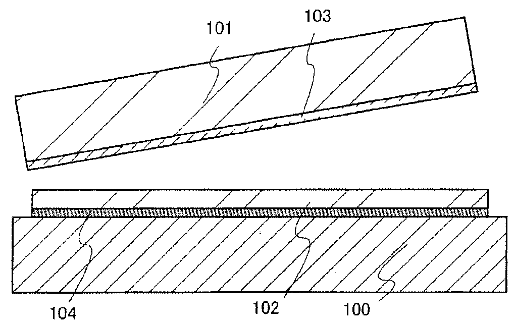
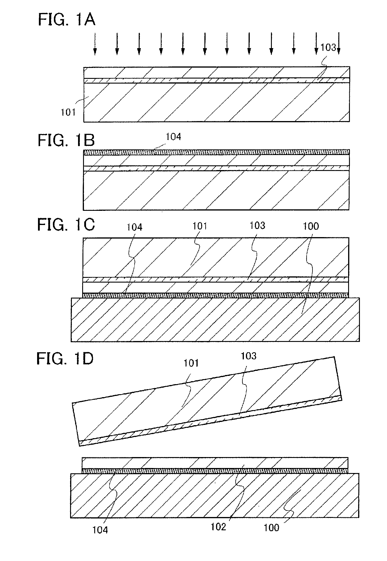
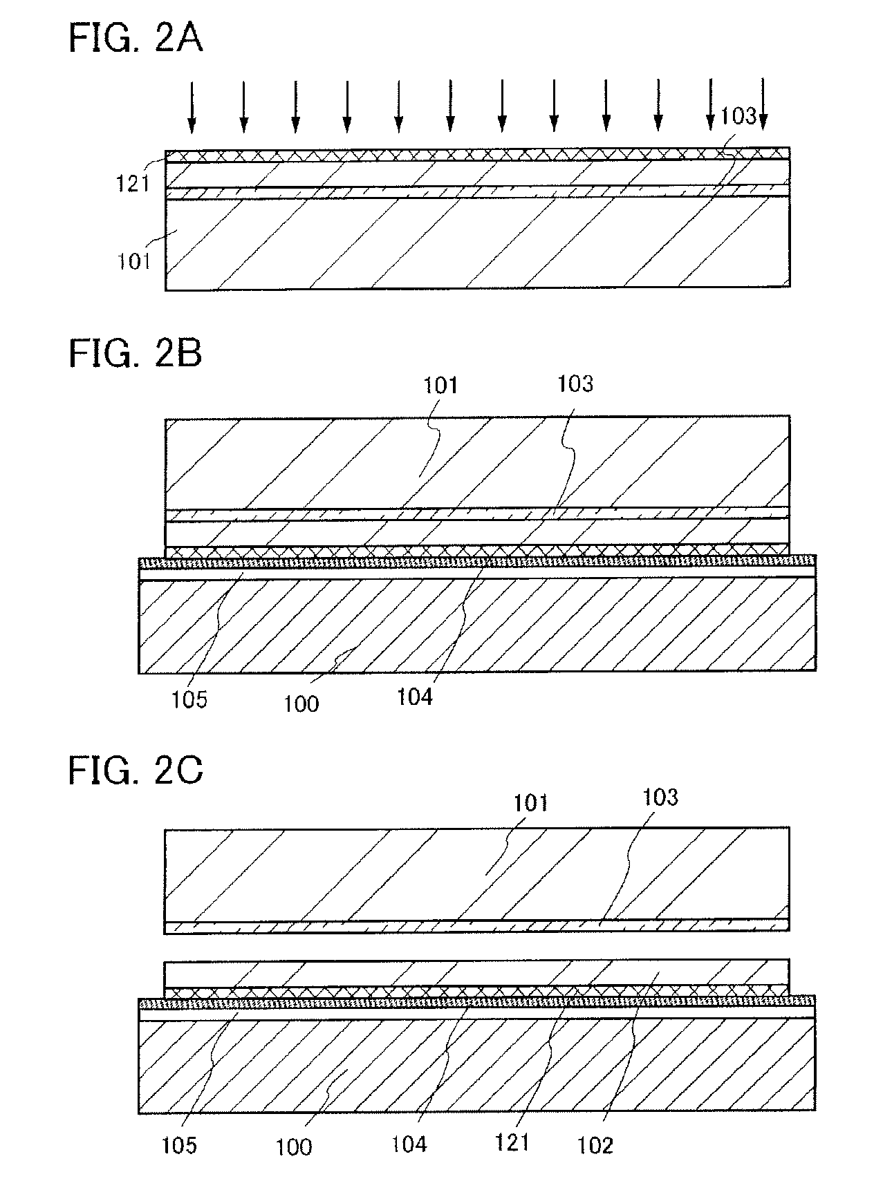
[0067]A manufacturing method of a semiconductor substrate according to the present invention will be described with reference to FIGS. 1A to 3B.
[0068]A semiconductor substrate 101 shown in FIG. 1A is cleaned, and irradiation with ions accelerated by electric field is conducted, so that a separation layer 103 is formed at a predetermined depth from a surface. Irradiation with the ions is carried out in consideration of the thickness of an LTSS layer to be transferred to a base substrate. The thickness of the LTSS layer is set at 5 to 500 nm, preferably 10 to 200 nm. The accelerating voltage at irradiation with ions is set in consideration of such a thickness; accordingly, the semiconductor substrate 101 is irradiated with the ions.
[0069]The separation layer may be formed by irradiation with ions by an ion doping method or an ion implantation method. The separation layer is formed by irradiation with ions of hydrogen, helium, or halogen typified by fluorine. In the case of irradiation...
embodiment mode 2
[0133]Embodiment Mode 2 will describe an example of manufacturing a semiconductor device using the LTSS layer that is formed over the glass substrate in Embodiment Mode 1. Specifically, a liquid crystal display device using a liquid crystal display element as a display element will be described. Note that repetitive descriptions for the same components as or components having similar functions to the components in Embodiment Mode 1 are omitted.
[0134]FIG. 16A is a top view showing a structure of a display panel according to the present invention. A pixel portion 2701 in which pixels 2702 are arranged in matrix, a scanning line input terminal 2703, and a signal line input terminal 2704 are formed over a substrate 2700 having an insulating surface. The number of pixels may be determined in accordance with various standards. In the case of XGA, the number of pixels may be 1024×768×3 (RGB). In the case of UXGA, the number of pixels may be 1600 1200×3 (RGB), and if the display panel is fo...
embodiment mode 3
[0196]A semiconductor device having a light-emitting element can be formed by applying the present invention, and the light-emitting element emits light by any one of bottom emission, top emission, and dual emission. Embodiment Mode 3 will describe an example of a manufacturing method of a semiconductor device in which a semiconductor device having a display function (also called a display device or a light-emitting device) is manufactured as a bottom-emission, dual-emission, or top-emission semiconductor device with high performance and high reliability with high yield, with reference to FIGS. 8A to 10.
[0197]A semiconductor device shown in FIGS. 8A and 8B employs a bottom-emission structure in which light is emitted in a direction indicated by an arrow. FIG. 8A is a plane view of the semiconductor device, and FIG. 8B is a cross sectional view taken along a line E-F of FIG. 8A. In FIGS. 8A and 8B, the semiconductor device includes an external terminal connection region 252, a sealin...
PUM
| Property | Measurement | Unit |
|---|---|---|
| temperature | aaaaa | aaaaa |
| temperature | aaaaa | aaaaa |
| temperature | aaaaa | aaaaa |
Abstract
Description
Claims
Application Information
 - Generate Ideas
- Intellectual Property
- Life Sciences
- Materials
- Tech Scout
- Unparalleled Data Quality
- Higher Quality Content
- 60% Fewer Hallucinations
Browse by: Latest US Patents, China's latest patents, Technical Efficacy Thesaurus, Application Domain, Technology Topic, Popular Technical Reports.
© 2025 PatSnap. All rights reserved.Legal|Privacy policy|Modern Slavery Act Transparency Statement|Sitemap|About US| Contact US: help@patsnap.com