Method of Manufacturing N-Type Multicrystalline Silicon Solar Cells

a multi-crystalline silicon and solar cell technology, applied in the field of solar cell manufacturing, can solve the problems of inability to maintain the quality of the thin film layer deposited on the substrate, no proper solution for integrating these two processes, and achieve the effect of increasing the current of the solar cell

Inactive Publication Date: 2008-11-20
STICHTING ENERGIEONDERZOEK CENT NEDERLAND
View PDF6 Cites 23 Cited by
  • Summary
  • Abstract
  • Description
  • Claims
  • Application Information

AI Technical Summary

Benefits of technology

[0011]The dielectric film is deposited on the phosphorus-diffused layer. With the dielectric film, the inside reflection at the back side is improved and the current of the solar cell is increased. Due to the annealing, a hydrogen passivation is carried out. This passivation step is carried out prior to the formation of the thin film heterojunction. Therefore, heating the p-type silicon thin film at higher temperatures than its deposition temperature can be avoided, and so the quality of the p-type silicon thin film is maintained.
[0012]Preferably, the dielectric comprises SiN. If silicon nitride (SiN) is adopted for the dielectric film, the SiN can protect the phosphorus-diffused layer from a NaOH solution and a dilute fluoric acid which may be used for the pre-treatment of the formation of the thin film heterojunction.

Problems solved by technology

However, there has been no proper solution for integrating these two processes into the manufacturing of a HIT structure in an n-type multicrystalline silicon substrate.
This is because the thin film layer deposited on the substrate, cannot maintain its quality with high temperature process like phosphorus diffusion or hydrogen passivation.

Method used


Image

  • Method of Manufacturing N-Type Multicrystalline Silicon Solar Cells
  • Method of Manufacturing N-Type Multicrystalline Silicon Solar Cells
  • Method of Manufacturing N-Type Multicrystalline Silicon Solar Cells

Examples


examples

[0032]Below, a further explanation of the invention is made using some other practical examples.

[0033]In a laboratory, 240 wafers with a thickness between 200-240 μm comprising a n-type mc-Si substrate with a resistivity of 0.5-3 ohm·cm were prepared. These wafers were sliced out from one square column with the size (width and depth) of 125×125 mm2, which was cut out from one casted ingot. The wafers were numbered #1 to #240 according to the position in the original ingot. They were divided into six groups wherein every sixth wafer was placed in a specific group. Each group had 40 wafers. Hereafter, the groups are referred to as group B, group C, group D, group E, group F, group G wherein:

Group B: #1, #7, #13, #235

Group C: #2, #8, #14, . . . , #236

Group D: #3, #9, #15, . . . , #237

Group E: #4, #10, #16, . . . , #238

Group F: #5, #11, #17, . . . , #239

Group G: #6, #12, #18, . . . , #240.

Example

Group B

[0034]Group B is a typical example of the invention. The solar cells structure shown ...

example

Results

[0042]The current-voltage characteristics of the completed cells were measured with a procedure described in IEC 60904. Table I shows the average values of the cell properties of each group, wherein Jsc is the short circuit current, Voc is the open circuit voltage and FF is the Fill Factor.

TABLE IHydrogenin SiNAnneal SiNJscVocEfficiencyGroupRemark[atomic %][° C.][mA / cm2][mV]FF [%][%]BTypical example7650-75032.661377.215.4CConventional HIT——29.659577.413.6DWithout back SiN——30.560577.114.2ELow H content SiN850-90031.860877.114.9FHigh H content SiN22650-75031.760877.214.9GWithout anneal SiN9—31.460777.214.7

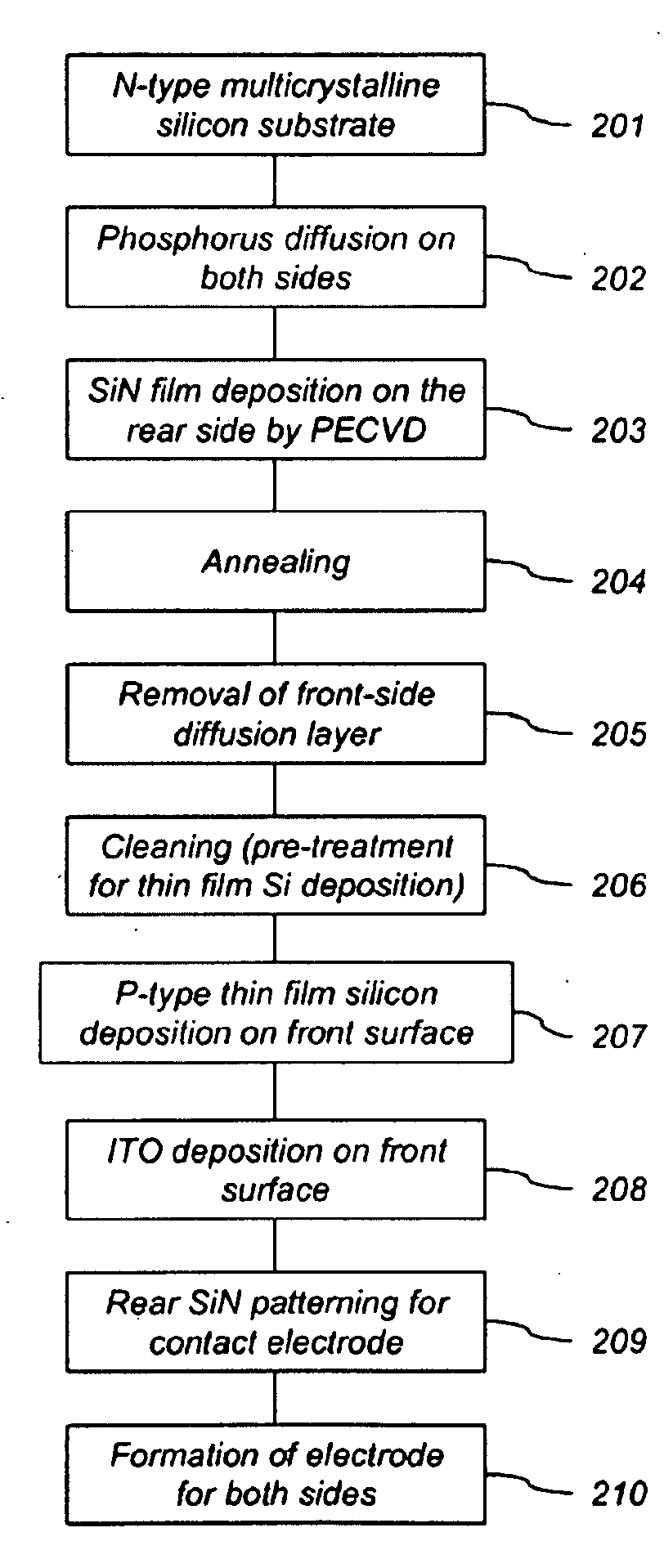
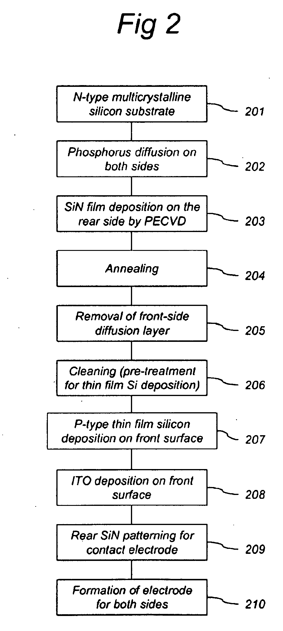
[0043]When comparing group D with group C, it shows that the short circuit current Jsc and the open circuit voltage Voc are improved. This is most certainly due to the presence of the back side phosphorus-doped layer 2. Because of the phosphorus diffusion process, see step 202 of FIG. 2, iron contamination present in the casted wafers is gettered by diffused phosphorus atoms ...


PUM


Abstract

The invention provides solar cells and methods of manufacturing solar cells having a Hetero-junction with Intrinsic Thin-layer (HIT) structure using an n-type multicrystalline silicon substrate. An n-type multicrystalline silicon substrate is subjected to a phosphorus diffusion step using a relatively high temperature. The front side diffusion layer is then removed. As a next step, a p-type silicon thin film is deposited at the front side of the substrate. This sequence avoids heating the p-type silicon thin film above its deposition temperature, and maintains the quality of the p-type silicon thin film.

Description

[0001]This application claims priority to Netherlands Application No. 1030200, filed Oct. 14, 2005, and International Application No. PCT / NL2006 / 050242 (Publication WO 2007 / 043881) which are incorporated herein by reference in their entirety.FIELD OF THE INVENTION[0002]The invention relates to the manufacture of solar cells. It more particularly relates to a method of manufacturing solar cells using an n-type multicrystalline silicon substrate.BACKGROUND[0003]Multicrystalline silicon (mc-Si) solar cells are usually made of p-type substrate because of its longer diffusion length of the minority carrier than n-type's. The silicon feedstock for the solar cell industry largely depends on the feedstock for the Integrated Circuit (IC) industry. This is because at the manufacture of silicon, the high quality silicon is reserved for the IC industry, and the lesser quality silicon forms the feedstock for the solar cell industry. Due to a recent shortage of the whole silicon feedstock, it is ...

Claims


Application Information

Patent Timeline
Patent Type & Authority Applications(United States)
IPC IPC(8): H01L31/00H01L21/00H01L31/0747
CPCH01L31/0747H01L31/18H01L31/1804H01L31/186H01L31/1868Y02E10/547Y02P70/50H01L31/072
Inventor KOMATSU, YUJIGOLDBACH, HANNO DIETRICHSCHROPP, RUDOLF EMMANUEL ISIDOREGEERLIGS, LAMBERT JOHAN
Owner STICHTING ENERGIEONDERZOEK CENT NEDERLAND
Why Eureka
Try Eureka