Coating composition for forming oxide film and method for producing semiconductor device using the same

a technology of coating composition and oxide film, which is applied in the direction of coatings, electrical appliances, basic electric elements, etc., can solve the problems of no success in improving the hardware of deposition apparatuses, reducing yield, and reducing the width of etching, so as to suppress the phenomenon of increased wet etching rate, low level, and low cost

Inactive Publication Date: 2008-12-11
ELPIDA MEMORY INC
View PDF0 Cites 48 Cited by
  • Summary
  • Abstract
  • Description
  • Claims
  • Application Information

AI Technical Summary

Benefits of technology

[0026]An exemplary object of the invention is to provide a coating composition for forming an oxide film, which can suppress the phenomenon of an increased wet etching rate caused by a part of the SOG film embedded inside a groove becoming low-density, and which can suppress the volume expansion coefficient to a low level, and a method for producing a semiconductor device using the same.
[0029]According to an exemplary aspect of the invention, a coating composition for forming an oxide film, which can suppress the phenomenon of an increased wet etching rate caused by a part of the SOG film embedded inside a groove becoming low-density, and which can suppress the volume expansion coefficient to a low level, and a method for producing a semiconductor device using the same can be provided.

Problems solved by technology

However, with the miniaturization of devices, trench widths are now heading towards dimensions below 60 nm.
If this hollow 411 is formed, short-circuiting occurs between the adjacent gates in the subsequent steps, thereby decreasing the yield.
Further, there has been no success in terms of improving the deposition apparatus hardware.
This problem does not only occur during STI formation, but is also commonly observed when a groove having a large aspect ratio is embedded with an SOG film and then subjected to a heat treatment of at least a certain temperature (about 600° C.).
For example, for the formation of a wiring interlayer dielectric film between DRAM gate electrodes (word lines), there is a demand for a lower temperature process (not more than 700° C.) and thus, for a device having a wiring interlayer interval at the 60 nm level, the BPSG (Boron Phosphorus Silicon Glass) used in related art cannot sufficiently reflow, whereby void formation becomes a problem like when forming an STI.
However, like when forming the STI, a part of the SOG film embedded inside the groove becomes low-density, so that the wet etching rate increases.
Thus, during the wet treatment by hydrofluoric acid and the like when forming a contact plug, the contact hole widens, which becomes a cause for short-circuiting between adjacent contact plugs.
On the other hand, from the measured results of FT-IR, the polysilazane SOG film embedded in the STI trench portion was almost completely SiO2, which makes it difficult to believe that any unreacted polysilazane remained.
As a result, it became clear that although they could suppress the phenomenon of a very high SOG film wet etching rate, the thermal oxide film 305 became thicker, thereby causing the semiconductor substrate device forming region to become narrower, and thus this method was not practical (FIG. 6).
With this method, although some effects were exhibited for grooves of a certain size, for relatively wide grooves the phenomenon of an increased wet etching rate could not be suppressed.
Further, it became clear that, depending on the groove, the way that stress is applied is different, which can cause unexpected effects on transistor properties such as threshold voltage and ON current.
As a result, although the phenomenon of an increased wet etching rate for the part of the SOG film embedded inside the groove could be suppressed, the formed SOG film had a large volume expansion coefficient, and the substrate curved in a convex manner, and thereby, there was a problem that delivery errors in the semiconductor manufacturing apparatus occurred.
Further, silicon crystals formed after the polysilane was heat treated and these crystals could not all be oxidized as is, which became a factor in problems such as an increased localized leak current.

Method used


Image

  • Coating composition for forming oxide film and method for producing semiconductor device using the same
  • Coating composition for forming oxide film and method for producing semiconductor device using the same
  • Coating composition for forming oxide film and method for producing semiconductor device using the same

Examples


example 1

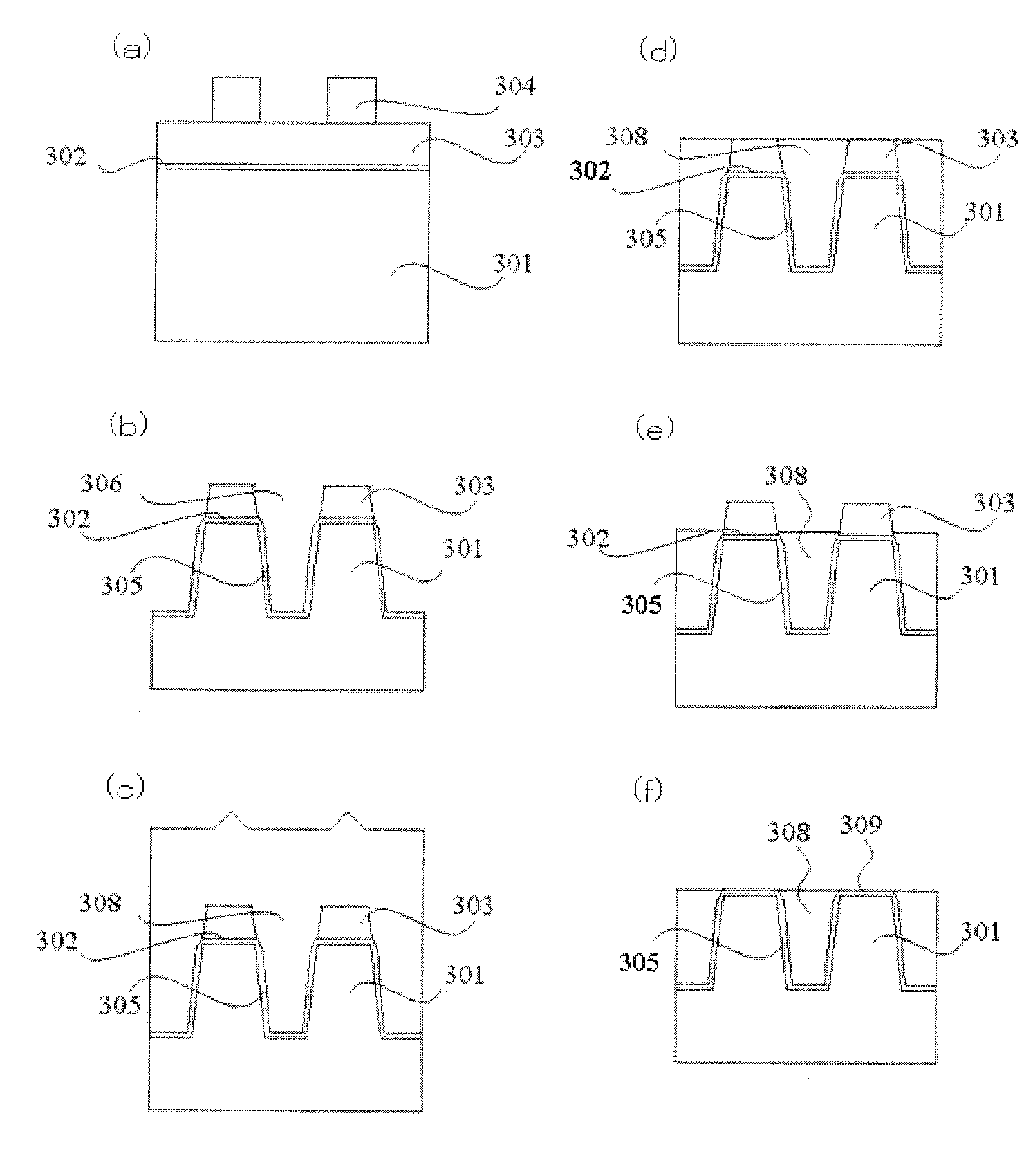
[0066]In Example 1, a device isolation region (STI) was formed on a semiconductor substrate using a coating composition for forming an oxide film which was a mixture of a polysilazane and a polysilane.

[0067]First, on a semiconductor substrate 101, a pad oxide film 102 (thickness: 9 nm) was formed by thermal oxidation and a nitride film 103 (thickness: 120 nm) was formed by LP-CVD. A pattern of photoresist 104 was formed on the nitride film 103 using a known lithography technique (FIG. 1(a)).

[0068]Next, with the photoresist 104 as a mask, the nitride film 103 and the pad oxide film 102 were patterned using a known etching technique. Then, the photoresist 104 was removed by ashing or the like in an oxygen plasma atmosphere. Next, with the patterned nitride film 103 as a mask, the semiconductor substrate 101 was etched to form a trench 106 (depth: about 180 nm) for device isolation. At this stage, the nitride film 103 was etched so that the thickness decreased from the original 120 nm ...

example 2

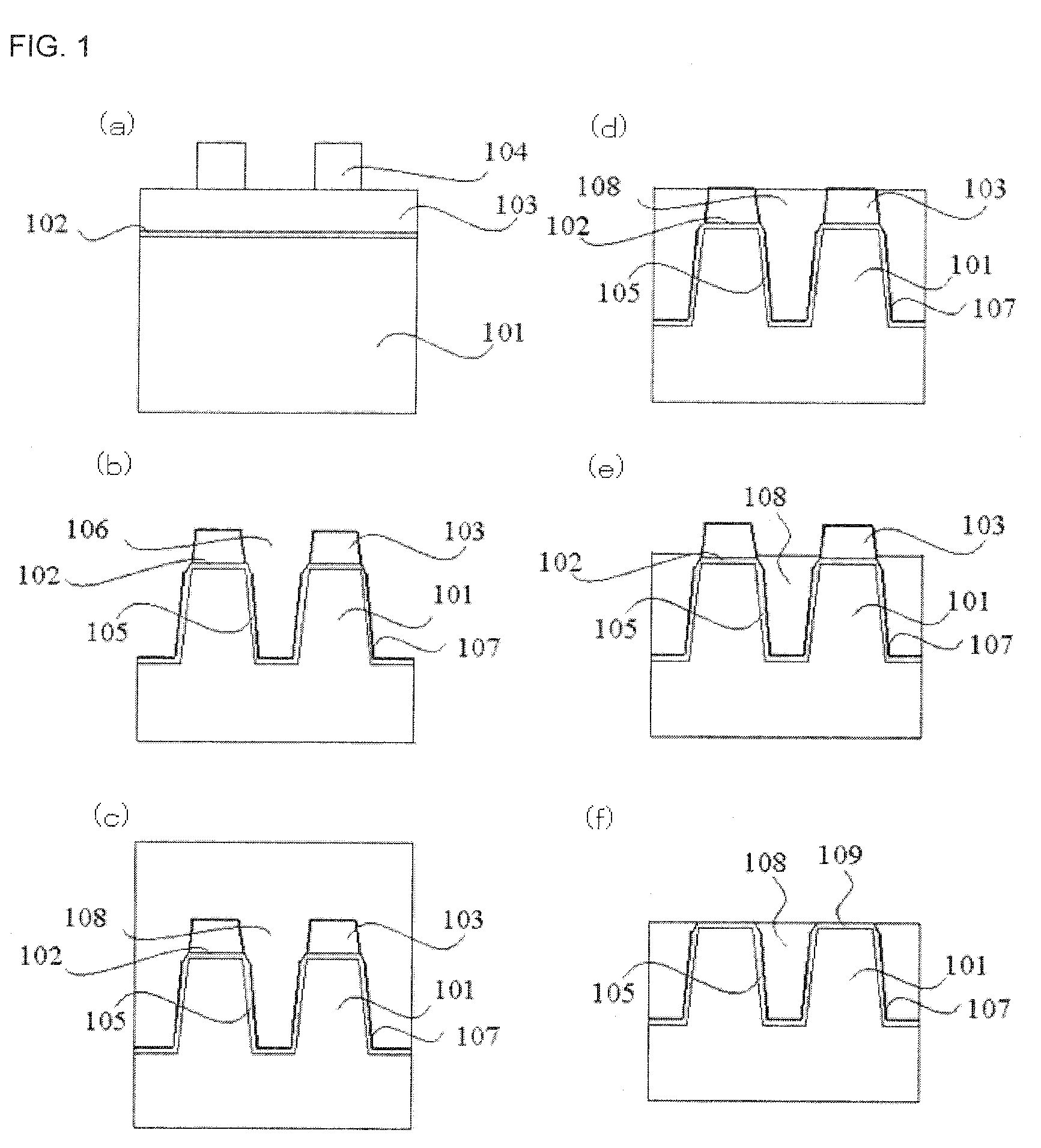
[0076]In Example 2, a gate interlayer dielectric film was formed using a coating composition for forming an oxide film which was a mixture of a polysilazane and a polysilane.

[0077]First, a gate interlayer dielectric film 202 was formed on a semiconductor substrate 201 having a formed device isolation region (not shown) such as STI. Next, a polysilicon 203 was formed on the gate interlayer dielectric film 202, and a metal electrode 204 of tungsten (W) or the like was formed on the polysilicon 203. It is noted that some works were carried out to suppress the interfacial resistance of a silicide and the like between the polysilicon 203 and the metal electrode 204. Further, a CVD nitride film 205 was formed on the metal electrode 204 (FIG. 2(a)).

[0078]Next, the CVD nitride film 205 and the metal electrode 204 were patterned using a known lithography technique and an etching technique (FIG. 2(b)).

[0079]Next, a nitride film 206 for preventing metal scattering was formed over the whole sur...

example 3

[0084]In Example 3, a device isolation region (STI) was formed on a semiconductor substrate using a coating composition for forming an oxide film which was a mixture of a hydrogenated silsesquioxane and a polysilane. Here, the method was carried out in the same manner as in Example 1, except that a solution prepared by mixing Type-12 (trade name; a hydrogenated silsesquioxane manufactured by Tokyo Ohka Kogyo Co., Ltd.) with cyclopentasilane in the same amount was used as the coating composition for forming an oxide film.

[0085]When this coating composition for forming an oxide film was coated on a non-patterned silicon substrate, then irradiated with UV light and subjected to a heat treatment, the volume change from after the baking of the formed film to after the thermal oxidation treatment was −3%. The oxide film embedded in the space portion between the gates formed thereby had an etching rate with hydrofluoric acid of roughly 1.1 times of the non-space portion (upper part of the ...


PUM

PropertyMeasurementUnit
thicknessaaaaaaaaaa
thicknessaaaaaaaaaa
depthaaaaaaaaaa

Abstract

A coating composition for forming an oxide film, which can suppress the phenomenon of an increased wet etching rate caused by a part of the SOG film embedded inside a groove becoming low-density, and which can suppress the volume expansion coefficient to a low level, and a method for producing a semiconductor device using the same are provided. An oxide film is formed inside a groove by: coating a coating composition for forming an oxide film, which contains a polysilazane or a hydrogenated silsesquioxane, and a polysilane, on a substrate having a groove; and thereafter heat treatment in an oxidizing atmosphere. This method is suitable for forming a device isolation region and a wiring interlayer dielectric film.

Description

BACKGROUND OF THE INVENTION[0001]1. Field of the Invention[0002]An exemplary aspect of the invention relates to a coating composition for forming an oxide film which constitutes a semiconductor substrate device isolation region or a wiring interlayer dielectric film, and a method for producing a semiconductor device using the same.[0003]2. Description of the Related Art[0004]Related art for forming a device isolation region (STI: Shallow Trench Isolation), in which a trench formed among the device forming regions of a semiconductor substrate is embedded with an insulator, will now be described with reference to FIG. 3.[0005]First, on a semiconductor substrate 301, a pad oxide film 302 (thickness: 9 nm) is formed by thermal oxidation and a nitride film 303 (thickness: 120 nm) is formed by LP-CVD. A photoresist 304 pattern is formed on the nitride film 303 using a known lithography technique (FIG. 3(a)).[0006]Next, with the photoresist 304 as a mask, the nitride film 303 and the pad o...

Claims


Application Information

Patent Timeline
Patent Type & Authority Applications(United States)
IPC IPC(8): H01L21/762C09D183/00
CPCC09D183/04C09D183/16H01L21/02164H01L21/02211H01L21/02216H01L21/02222H01L21/02282H01L21/02323H01L21/02337H01L21/02348H01L21/3121H01L21/3124H01L21/3125H01L21/316C08L83/00
Inventor HIROTA, TOSHIYUKI
Owner ELPIDA MEMORY INC
Why Eureka
Try Eureka