Squarylium dye, method of producing the same, photoelectric conversion element containing the dye, and solid-state imaging device

a technology of squarylium dye and photoelectric conversion element, which is applied in the field of squarylium dye, can solve the problems of inability to achieve satisfactory control of absorption spectrum, inability to selectivity, and large size of device or apparatus, etc., and achieves strong absorption and large absorption intensity

Active Publication Date: 2008-12-18
FUJIFILM CORP
View PDF4 Cites 23 Cited by
  • Summary
  • Abstract
  • Description
  • Claims
  • Application Information

AI Technical Summary

Benefits of technology

[0014]An object of the present invention is to provide a squarylium dye having strong absorption in the near infrared region and having only relatively small absorption in the visible region, which can be vapor-deposited without causing decomposition in the vapor deposition process and enables the production of a vapor-deposited film free of contamination, and further provide a good near infrared-absorbing organic thin film using the dye, which exhibits a large absorption intensity in the near infrared region of 700 nm or more in the thin-film absorption characteristics and exhibits only an absorption intensity of 1 / 10 or less of the near infrared absorption in all wavelengths of 400 to 550 nm.

Problems solved by technology

However, the materials described in either publication are in principle unable to favor wavelength selectivity, because the film formed has a broad absorption spectrum and the photoelectric conversion spectrum indicative of the wavelength dependency of photoelectric conversion ability becomes broad.
A squarylium dye has been intensively studied as an electrophotographic material because of its characteristic sharp absorption spectrum and good photoelectric conversion properties, but satisfactory control of the absorption spectrum is not possible.
According to such a method, an image of visible light and an image of infrared light may be obtained at the same time, but these methods have problems, for example, that: the size of the device or apparatus becomes large and the cost rises; the image is not sampled at the same point and the synthesis, processing and the like of image information are difficult; or the color filter is transparent only to light at a limited wavelength and the non-transmitted light is not utilized, giving rise to bad light utilization efficiency.
The system of stacking, in the vertical direction, a photoelectric conversion part for detecting infrared light and a photoelectric conversion part for detecting visible light is disadvantageous not only in that the absorption ranges of respective portions are overlapped in the depth direction of the silicone substrate to give bad spectral characteristics and the color separation is originally poor, but also in that although it is necessary in the case of using Si to further provide a photoelectric conversion part for detecting infrared light as a lowermost layer of the silicon substrate in the sensor of U.S. Pat. No. 5,965,875, infrared light is absorbed by the upper layer to reduce the infrared light reaching the lowermost layer inside of the silicon substrate and the sensitivity decreases.
However, according to the studies by the present inventors, use of a phthalocyanine-based material is disadvantageous in that a high photoelectric conversion efficiency can be hardly exerted in a wide wavelength region.
The squarylium-based dye generally decomposes at the vapor deposition and therefore, it is difficult to produce an element having high performance.
359 (1988)), but application of this system is limited to an electrophotographic system.

Method used


Image

  • Squarylium dye, method of producing the same, photoelectric conversion element containing the dye, and solid-state imaging device
  • Squarylium dye, method of producing the same, photoelectric conversion element containing the dye, and solid-state imaging device
  • Squarylium dye, method of producing the same, photoelectric conversion element containing the dye, and solid-state imaging device

Examples


first embodiment

of Photoelectric Conversion Element

[0182]FIG. 11 is a cross-sectional schematic view roughly showing the construction of the photoelectric conversion element in the first embodiment of the present invention.

[0183]The photoelectric conversion element shown in FIG. 11 comprises at least a photoelectric conversion part A containing a lower electrode 11, an upper electrode 13 facing the lower electrode 11, and a photoelectric conversion film 12 provided between the lower electrode 11 and the upper electrode 13. The photoelectric conversion element shown in FIG. 11 is used by making light incident from the upper side of the upper electrode 13.

[0184]The upper electrode 13 is a transparent electrode composed of an electrically conductive material transparent to light (visible light and infrared light) in the combined range of a visible region and an infrared region (the range at a wavelength of 400 nm or more). A bias voltage is applied to the upper electrode 13 through wiring not shown. T...

second embodiment

of Photoelectric Conversion Element

[0199]FIG. 12 is a cross-sectional schematic view roughly showing the construction of the photoelectric conversion element in the second embodiment of the present invention.

[0200]The photoelectric conversion element shown in FIG. 12A comprises a semiconductor substrate K such as silicon, a visible light photoelectric conversion part B stacked on the upper side of the semiconductor substrate K, and the photoelectric conversion part A shown in FIG. 11 stacked on the upper side of the visible light photoelectric conversion part B.

[0201]The visible light photoelectric conversion part B has almost the same construction as the photoelectric conversion part A and as for the organic photoelectric conversion material constituting the photoelectric conversion film 12 of the photoelectric conversion part A, a material having an absorption peak in the visible region of the absorption spectrum in the combined range of a visible region and an infrared region (th...

third embodiment

of Photoelectric Conversion Element

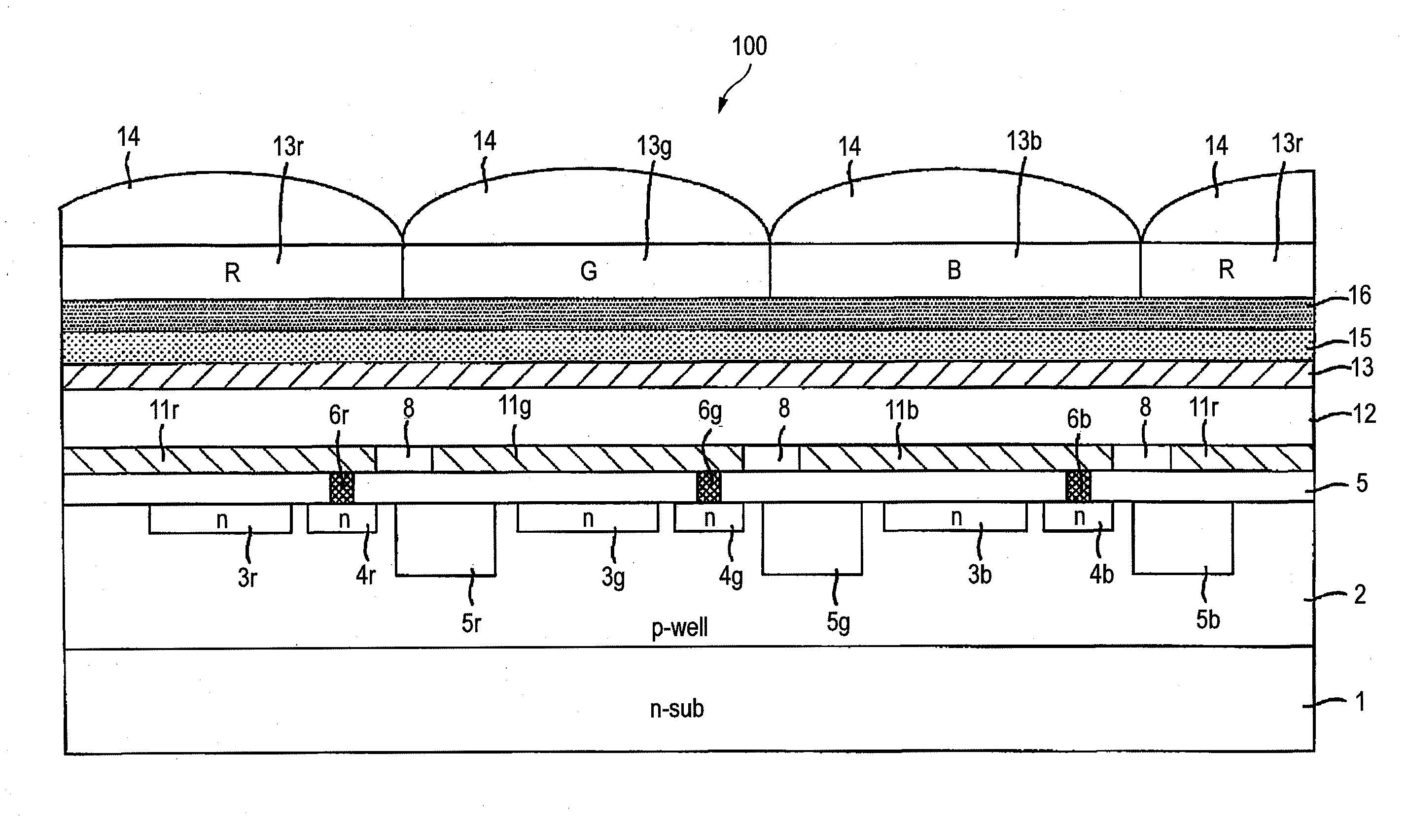
[0250]In this embodiment, a construction of realizing a solid-state imaging device by using the photoelectric conversion element having a construction shown in FIG. 12B is described.

[0251]FIG. 14 is a partial surface schematic view of an imaging device for explaining the embodiment of the present invention, and FIG. 15 is a cross-sectional schematic view cut along the A-A line of the imaging device shown in FIG. 14. In FIG. 14, illustration of a microlens 14 is omitted. Also, in FIG. 15, the same constituents as those in FIG. 11 are denoted by like reference numerals.

[0252]A p-well layer 2 is formed on an n-type silicon substrate 1. In the following, the n-type silicon substrate 1 and the p-well layer 2 are collectively referred to as a semiconductor substrate. In the row direction and the column direction crossing with the row direction at right angles on the same plane above the semiconductor substrate, three kinds of color filters, that is, a co...


PUM

PropertyMeasurementUnit
decomposition initiating temperatureaaaaaaaaaa
absorption maximum wavelengthaaaaaaaaaa

Abstract

A squarylium dye represented by formula (1):
wherein A1 and B1 each independently represents a ring structure, and R1 and R2 each independently represents a substituent having a carbon number of 1 to 12.

Description

BACKGROUND OF THE INVENTION[0001]1. Field of the Invention[0002]The present invention relates to a squarylium dye having absorption in the near infrared part and a method of producing the same. The present invention also relates to a photoelectric conversion element having a photoelectric conversion part containing a pair of electrodes and an infrared organic photoelectric conversion film which contains the squarylium dye and is provided between the pair of electrodes, and a solid-state imaging device.[0003]2. Background Art[0004]With recent progress of organic electronics, an element using an organic dye thin film has been involved in intensive development. As one of these elements, an element using an organic material for the photoelectric conversion film is actively studied, typically including an electrophotographic device and a solar cell, and studies on various materials therefore are being made. For example, the electrophotographic material includes those described in Kock-Ye...

Claims


Application Information

Patent Timeline
Patent Type & Authority Applications(United States)
IPC IPC(8): H01L31/0216C07D403/02
CPCC07D209/12C07D209/60H01L27/14643H01L51/0064H10K85/652
Inventor NOMURA, KIMIATSUKITAMURA, TETSUMITSUI, TETSURO
Owner FUJIFILM CORP
Why Eureka
Try Eureka