Semiconductor device and method for manufacturing semiconductor device

a semiconductor and semiconductor technology, applied in the direction of semiconductor devices, electrical devices, transistors, etc., can solve the problems of increasing junction leakage, achieve the effect of reducing junction leakage, reducing stress variation, and improving semiconductor device characteristics

Active Publication Date: 2009-01-01
SONY CORP
View PDF3 Cites 21 Cited by
  • Summary
  • Abstract
  • Description
  • Claims
  • Application Information

AI Technical Summary

Benefits of technology

[0011]Furthermore, in a MOS transistor, the layout area can be decreased by employing a structure in which a diffusion layer of opposite conductivity type is disposed adjacent to one of source and drain regions, and one of source and drain regions and the diffusion layer of opposite conductivity type are short-circuited by a silicide layer disposed as a surface layer. In such a structure, in the case where epitaxial layers composed of silicon germanium (SiGe) are used for source / drain regions of a PMOS transistor, an n-type diffusion layer formed by diffusing an n-type impurity, such as arsenic (As) or phosphorus (P), in a surface layer of a semiconductor substrate is provided as a diffusion layer of opposite conductivity type.
[0012]However, the diffusion rate of the n-type impurity in SiGe is higher than in a semiconductor substrate composed of silicon, i.e., in the case of arsenic (As), about seven times higher, and in the case of phosphorus (P), about two times higher. Consequently, the n-type impurity in the diffusion layer of opposite conductivity type (n-type diffusion layer) is diffused into the adjacent source / drain regions (epitaxial layers composed of SiGe) and easily reaches the channel region, thus increasing the threshold of the MOS transistor.
[0013]It is desirable to provide a semiconductor device including epitaxial layers, the depth of which is controlled without depending on the layout, and in which crystal defects are prevented from occurring, thus enabling improvement in characteristics, and to provide a method for manufacturing the semiconductor device.
[0016]In the semiconductor device and the method for manufacturing the semiconductor device according to the embodiments of the present invention, the source / drain regions include the epitaxial layers and the diffusion layers. Consequently, the width of the epitaxial layers is adjusted by changing the width of the diffusion layers. Thus, without depending on the layout, the width of the recessed portions of the semiconductor substrate, in which the epitaxial layers are to be formed, is controlled, and the depth of the recessed portions recessed by etching is controlled. Consequently, for example, by setting the width of the epitaxial layers to be a predetermined value by changing the width of the diffusion layers, the depth of the recessed portions of the semiconductor substrate in which the epitaxial layers are disposed is equalized, without depending on the layout. Furthermore, since the formation area (layout area) of the epitaxial layers is reduced by portions corresponding to the diffusion layers, without depending on the layout, it is possible to obtain epitaxial layers having a small number of crystal defects.
[0017]As described above, according to the embodiments of the present invention, the depth of the recessed portions of the semiconductor substrate in which the epitaxial layers are disposed can be controlled without depending on the layout. Consequently, it is possible to suppress the variation in stress applied to channel regions beneath gate electrodes by the epitaxial layers with controlled depth. Furthermore, since epitaxial layers having a small number of crystal defects can be obtained without depending on the layout, junction leakage can be reduced. As a result, the characteristics of the semiconductor device can be improved.

Problems solved by technology

Furthermore, with respect to an epitaxial layer composed of silicon germanium (SiGe), as the layout area increases, the number of crystal defects increases, resulting in an increase in junction leakage.

Method used


Image

  • Semiconductor device and method for manufacturing semiconductor device
  • Semiconductor device and method for manufacturing semiconductor device
  • Semiconductor device and method for manufacturing semiconductor device

Examples


first embodiment

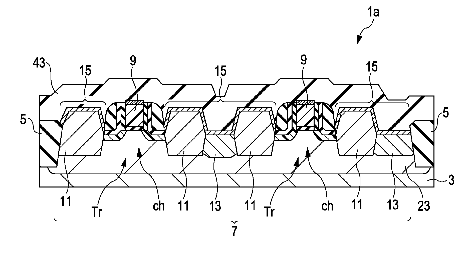
[0030]FIG. 1 is a schematic cross-sectional view showing a structure of a semiconductor device according to a first embodiment. In a semiconductor device 1a shown in FIG. 1, a surface of a semiconductor substrate 3 composed of silicon (Si) is isolated by isolation films 5, and gate electrodes 9 are disposed so as to extend across an isolated active region 7. At both sides of the gate electrodes 9, the surface of the semiconductor substrate 3 is recessed. Epitaxial layers 11 composed of a semiconductor material having a different lattice constant from that of the semiconductor substrate 3 are disposed in the recessed portions, and impurities are diffused into the epitaxial layers 11. Furthermore, with respect to the gate electrodes 9, diffusion layers 13 are disposed outside the epitaxial layers 11, the diffusion layers 13 being formed by diffusing impurities into a surface layer of the semiconductor substrate 3.

[0031]In the first embodiment, at both sides of the gate electrodes 9, t...

second embodiment

[0098]FIG. 6 is a schematic cross-sectional view showing a structure of a semiconductor device according to a second embodiment of the present invention. A semiconductor device 1b shown in FIG. 6 has the same structure as the semiconductor device 1a shown in FIG. 1 according to the first embodiment except that the depth of diffusion layers 13 constituting source / drain regions 15 is larger than the depth of epitaxial layers 11.

[0099]In the semiconductor device 1b having such a structure, by increasing the depth of the diffusion layers 13 located outside the epitaxial layers 11 with respect to the gate electrodes 9, in addition to the effect of the first embodiment, while reducing the short channel effect, the electric field of the depletion layer at the p-n junction can be reduced, and thus junction leakage can be further improved. Furthermore, by increasing the depth of the diffusion layers 13, the substrate impurity concentration at the junction is decreased. Consequently, the junc...

third embodiment

[0100]FIG. 7 is a schematic cross-sectional view showing a structure of a semiconductor device according to a third embodiment of the present invention. A semiconductor device 1c shown in FIG. 7 has the same structure as the semiconductor device 1a shown in FIG. 1 according to the first embodiment except that the height of the surface of the diffusion layers 13 constituting the source / drain regions 15 is lower than the height of the surface of the semiconductor substrate 3 beneath the gate electrodes 9.

[0101]In the semiconductor device 1c having such a structure, the stress film 43 covering the transistors Tr is extended to the position lower than the channel regions ch. Thereby, in addition to the effect of the first embodiment, the effect of application of stress to the channel regions ch by the stress film 43 can be enhanced.


PUM


Abstract

A semiconductor device includes a gate electrode disposed on a semiconductor substrate and source / drain regions disposed at both sides of the gate electrode, the source / drain regions being formed by implanting impurities. The source / drain regions include an epitaxial layer formed by epitaxially growing a semiconductor material having a different lattice constant from that of the semiconductor substrate in a recessed position at a side of the gate electrode, and a diffusion layer disposed in a surface layer of the semiconductor substrate.

Description

CROSS REFERENCES TO RELATED APPLICATIONS[0001]The present invention contains subject matter related to Japanese Patent Application JP 2007-169023 filed in the Japanese Patent Office on Jun. 27, 2007, the entire contents of which are incorporated herein by reference.BACKGROUND OF THE INVENTION[0002]1. Field of the Invention[0003]The present invention relates to semiconductor devices and methods for manufacturing semiconductor devices. More particularly, the invention relates to a semiconductor device in which semiconductor materials having different lattice constants are epitaxially grown in recessed portions at the sides of gate electrodes and a method for manufacturing the same.[0004]2. Description of the Related Art[0005]In semiconductor devices provided with MOS transistors, techniques that improve carrier mobility by application of stress to channel regions of a semiconductor substrate have been actively used. As one of such techniques, use of a structure shown in FIG. 11 has be...

Claims


Application Information

Patent Timeline
Patent Type & Authority Applications(United States)
IPC IPC(8): H01L21/336H01L29/78
CPCH01L21/823807H01L21/823814H01L29/665H01L29/6656H01L29/66431H01L29/7834H01L29/7843H01L29/7848H01L29/66636H01L21/20H01L21/18H01L27/088H01L29/0847H01L29/165H01L29/41783H01L29/45H01L29/7835
Inventor MATSUMOTO, TAKUJI
Owner SONY CORP
Why Eureka
Try Eureka