METHODS OF FABRICATING NANOSTRUCTURED ZnO ELECTRODES FOR EFFICIENT DYE SENSITIZED SOLAR CELLS

a technology of zno electrodes and solar cells, applied in the direction of polycrystalline material growth, semiconductor/solid-state device details, radiation control devices, etc., can solve the problems of low energy conversion efficiency, low cost of producing such high-purity silicon, and solar energy is still not able to fully compete with fossil fuel energy sources. , to achieve the effect of high energy conversion efficiency in optoelectronics, high surface area and plant-like morphologies

Inactive Publication Date: 2009-01-08
UNIV OF UTAH RES FOUND
View PDF6 Cites 7 Cited by
  • Summary
  • Abstract
  • Description
  • Claims
  • Application Information

AI Technical Summary

Benefits of technology

[0007]The present invention provides methods of forming metal oxide semiconductor nanostructures and, in particular zinc oxide (ZnO) semiconductor nanostructures, possessing high surface area, plant-like morphologies on a variety of substrates. The unique physical characteristics of the nanostructures make them particularly attractive for use as the electrodes in a variety of optoelectronic devices. In contrast to sintered nanoparticle-based optoelectronic devices, such as solar cells, the direct electrical pathways provided by the present nanostructures ensure the rapid collection of carriers generated throughout the material. As a result, the present nanostructures provide high energy conversion efficiencies in optoelectronics. In addition to providing unique electrode morphologies, the methods of the present invention use lower processing temperatures than other available methods.

Problems solved by technology

However, because of the continuously increasing cost of fossil fuel, and concerns about global warming, the importance of developing alternative energy sources has greatly increased.
Although interest in solar energy is increasing, solar energy is still not able to compete fully with fossil fuel energy sources because of a number of material challenges.
The cost of producing such high-purity silicon is significant.
Coupled with low energy conversion efficiency, the cost of power produced by these cells is still several times more than power produced by conventional energy sources.
Because of these issues, the current major challenge in this field is to radically reduce the overall cost of delivered solar electricity by significantly lowering the cost of the cell and improving its energy conversion efficiency.
This is a slow transport mechanism that limits device efficiency, especially at longer (less energetic) wavelengths, because recombination events become more likely.

Method used


Image

  • METHODS OF FABRICATING NANOSTRUCTURED ZnO ELECTRODES FOR EFFICIENT DYE SENSITIZED SOLAR CELLS
  • METHODS OF FABRICATING NANOSTRUCTURED ZnO ELECTRODES FOR EFFICIENT DYE SENSITIZED SOLAR CELLS
  • METHODS OF FABRICATING NANOSTRUCTURED ZnO ELECTRODES FOR EFFICIENT DYE SENSITIZED SOLAR CELLS

Examples


example 1

Formation of ZnO Nanostructures on Glass

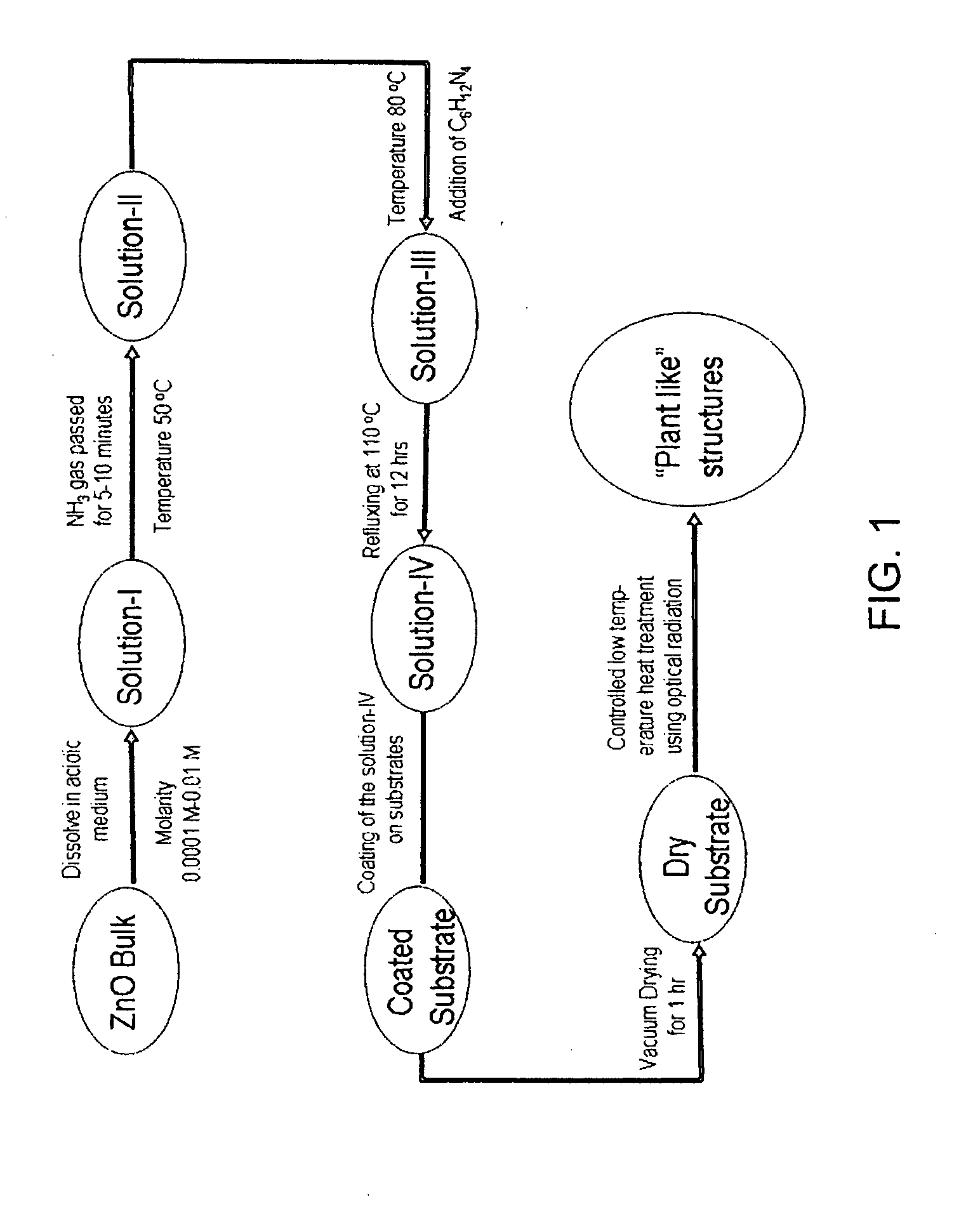
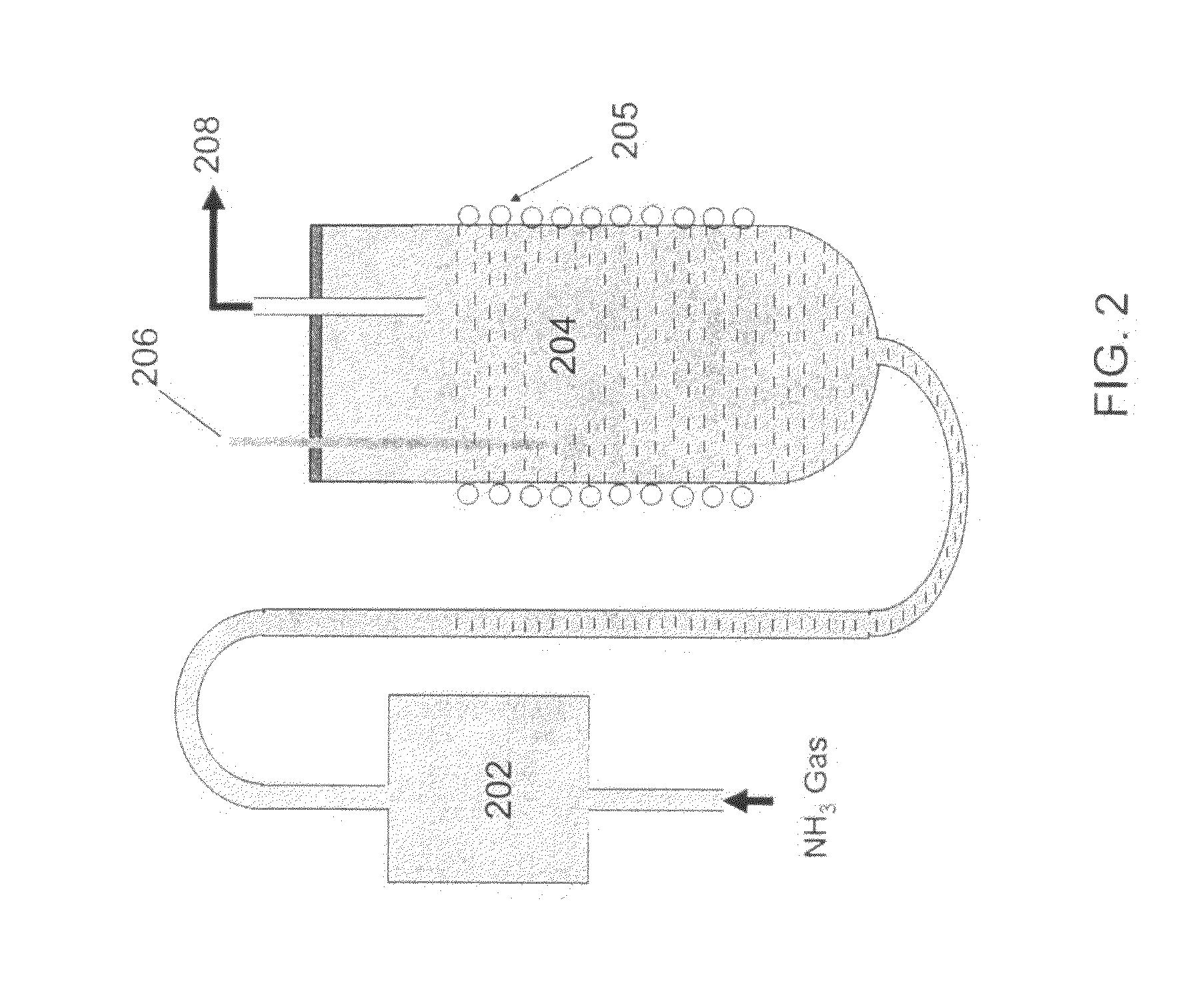
[0044]About 10 μL of solution-IV (see FIG. 1) having [ZnO]=0.001 M was spin-coated onto a 1-cm2 glass substrate. The coated substrate was uniformly illuminated using the arrangement shown in FIG. 3 with an incandescent light bulb light source. The optical fluence was 10 Watt / cm2, and the time of illumination was 20 minutes. The local temperature attained at the top of the substrate was 170° C. A scanning electron microscope (SEM) image of the ZnO nanostructures on glass is shown in FIG. 7.

example 2

Formation of ZnO Nanostructures on Si(111)

[0045]About 10 μL of solution-IV (see FIG. 1) having [ZnO]=0.01 M was spin-coated onto a 1 cm2 Si(111) substrate. The coated substrate was uniformly illuminated using the arrangement shown in FIG. 3 with an incandescent light bulb light source. The optical fluence was 14 Watt / cm2, and the time of illumination was 20 minutes. The local temperature attained at the top of the substrate was 150° C. FIG. 8 shows an SEM image of the resulting ZnO nanostructures.

example 3

Formation of ZnO Nanostructures on Sapphire (0001)

[0046]About 10 μL of solution-IV (see FIG. 1) having [ZnO]=0.0005 M was spin-coated onto a 1-cm2 sapphire (0001) substrate. The coated substrate was uniformly illuminated using the arrangement shown in FIG. 3 with an incandescent light bulb light source. The optical fluence was 16 Watt / cm2, and the time of illumination was 20 minutes. The local temperature attained at the top of the substrate was 170° C. FIG. 9 shows an SEM image of the resulting ZnO nanostructures.


PUM

PropertyMeasurementUnit
diameteraaaaaaaaaa
widthaaaaaaaaaa
widthaaaaaaaaaa

Abstract

The present invention provides methods of forming metal oxide semiconductor nanostructures and, in particular, zinc oxide (ZnO) semiconductor nanostructures, possessing high surface area, plant-like morphologies on a variety of substrates. Optoelectronic devices, such as photovoltaic cells, incorporating the nanostructures are also provided.

Description

FIELD OF THE INVENTION[0001]The present invention relates to metal oxide electrodes, photovoltaic cells incorporating the electrodes, and methods for making the electrodes. The present metal oxide electrodes possess plant-like morphology, may be made at low-temperatures on a variety of substrates, and exhibit improved conversion efficiency relative to more conventional electrodes.BACKGROUND OF THE INVENTION[0002]In recent years, research into nanotechnology and nanomanufacturing has been increasing. Of particular interest are nanostructured electrode materials, which may be used in unconventional energy sources such as dye sensitized solar cells, solid oxide fuel cells, and microbial fuel cells.[0003]More than seventy percent of the total power consumed in the world is produced by burning fossil fuel. However, because of the continuously increasing cost of fossil fuel, and concerns about global warming, the importance of developing alternative energy sources has greatly increased. S...

Claims


Application Information

Patent Timeline
Patent Type & Authority Applications(United States)
IPC IPC(8): H01L29/22H01L21/34H01L31/0296
CPCB82Y30/00C01G9/02C01P2004/03C01P2004/64Y02E10/542H01G9/204H01G9/2059Y02E10/52C01P2006/40Y10S977/723Y10S977/782Y10S977/811
Inventor TIWARI, ASHUTOSHSNURE, MICHAEL R.
Owner UNIV OF UTAH RES FOUND
Why Eureka
Try Eureka