

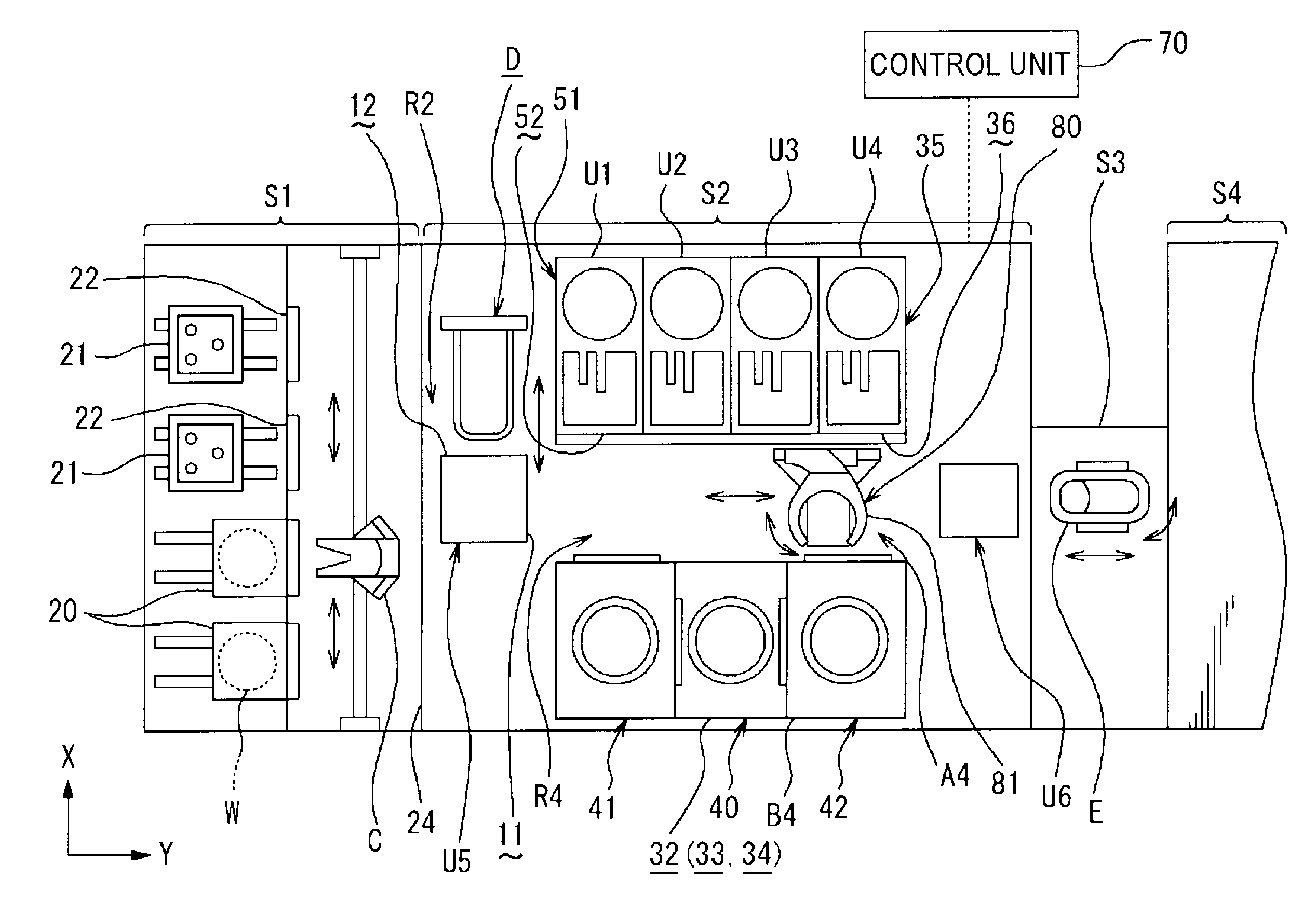
Substrate processing apparatus
a processing apparatus and substrate technology, applied in the direction of photomechanical equipment, instruments, vacuum evaporation coating, etc., can solve the problems of uniform coating film thickness, reduced apparatus operation rate, and inability to make uniform coating film thickness, etc., to reduce apparatus operation rate, eliminate airflow, and effective use of gas
- Summary
- Abstract
- Description
- Claims
- Application Information
AI Technical Summary
Benefits of technology
Problems solved by technology
Method used
Image

Examples
first embodiment
[0073]FIG. 5 is a schematic sectional view showing a first embodiment of the substrate processing apparatus according to the present invention, and FIG. 6 is a schematic sectional view of FIG. 5.
[0074]A coating unit 32A that is the substrate processing apparatus of the first embodiment includes a treatment chamber 40 for performing coating treatment to form a coating film (a resist film) of the wafer W, a pre-processing chamber 41 for cooling the wafer W before the coating treatment to a predetermined temperature, for example, 23° C., and a post-processing chamber 42 for heating the wafer W after the coating treatment to a predetermined temperature, for example, 100° C. to evaporate a remaining solvent in the resist film, are connected with the treatment chamber 40 being located at the middle. Further, the treatment chamber 40, the pre-processing chamber 41 and the post-processing chamber 42 are provided with transfer in / out ports 43a and 43b for the wafer W. At the transfer in / out ...
second embodiment
[0093]FIG. 7 is a schematic sectional view showing a second embodiment of the substrate processing apparatus according to the present invention.
[0094]A coating unit 32B that is the substrate processing apparatus of the second embodiment is a case in which the post-processing chamber 42 is placed on top of the pre-processing chamber 41 in the first embodiment, and the pre-processing chamber 41 and the post-processing chamber 42 are connected to the treatment chamber 40. In this case, the treatment chamber 40, the pre-processing chamber 41 and the post-processing chamber 42 are provided with transfer in / out ports 43a and 43b for the wafer W. At the transfer in / out ports 43a and 43b, shutters 44a and 44b for opening / closing the transfer in / out ports 43a and 43b are provided respectively. In one of the treatment chamber 40, the pre-processing chamber 41 and the post-processing chamber 42 (the treatment chamber 40 is shown in the drawing), a transfer arm 45c is disposed for delivering th...
third embodiment
[0101]FIG. 8 is a schematic sectional view showing a third embodiment of the substrate processing apparatus according to the present invention.
[0102]A coating unit 32C that is the substrate processing apparatus of the third embodiment is a case in which the treatment chamber 40 in the first embodiment is connected to a thermal processing chamber 49 housing a heating plate 58 and a cooling plate 56A. In this case, the thermal processing chamber 49 and the treatment chamber 40 are provided with a transfer in / out port 43c for the wafer W and a shutter 44c for opening / closing the transfer in / out port 43c. In one of the thermal processing chamber 49 and the treatment chamber 40, a transfer arm 45d is disposed for delivering the wafer W between the thermal processing chamber 49 and the treatment chamber 40.
[0103]In the thermal processing chamber 49, the heating plate 58 that is a heating means for heating the wafer W coated with the resist solution to a predetermined temperature (100° C.)...
PUM
| Property | Measurement | Unit |
|---|---|---|
| Fraction | aaaaa | aaaaa |
| Temperature | aaaaa | aaaaa |
| Concentration | aaaaa | aaaaa |
Abstract
Description
Claims
Application Information