Semiconductor device and method for manufacturing the same

a semiconductor and semiconductor technology, applied in the direction of semiconductor/solid-state device details, resistor housing/enclosement/embedding, resistive material coating, etc., can solve the problems of high frequency characteristics deterioration of parasitic capacitance between the substrate and the resistor, remarkable degradation of analog characteristics in the integrated circuit handling analog signals, and fluctuation of resistance value. , to achieve the effect of suppressing the resistance change ratio, less fluctuation of resistance value, and low parasitic capa

Inactive Publication Date: 2009-01-15
HITACHI LTD
View PDF5 Cites 17 Cited by
  • Summary
  • Abstract
  • Description
  • Claims
  • Application Information

AI Technical Summary

Benefits of technology

[0017]Since a resistor composed of nitrogen and tantalum as the main constituent elements and capable of suppressing the resistance change ratio to less than 1% even when a thermal load in the int

Problems solved by technology

Accordingly, since the resistor is formed at a position nearer to a substrate than the interconnection composed of a metal film, this results in a problem of generating parasitic capacitance between the substrate and the resistor to deteriorate high frequency characteristics.
However, the resistor including the metal film involves a problem that the resistance value fluctuates in accordance with the thermal hysteresis in the subsequent interconnection step.
Specifically, when an interconnection is formed after forming the resi

Method used


Image

  • Semiconductor device and method for manufacturing the same
  • Semiconductor device and method for manufacturing the same
  • Semiconductor device and method for manufacturing the same

Examples


first embodiment

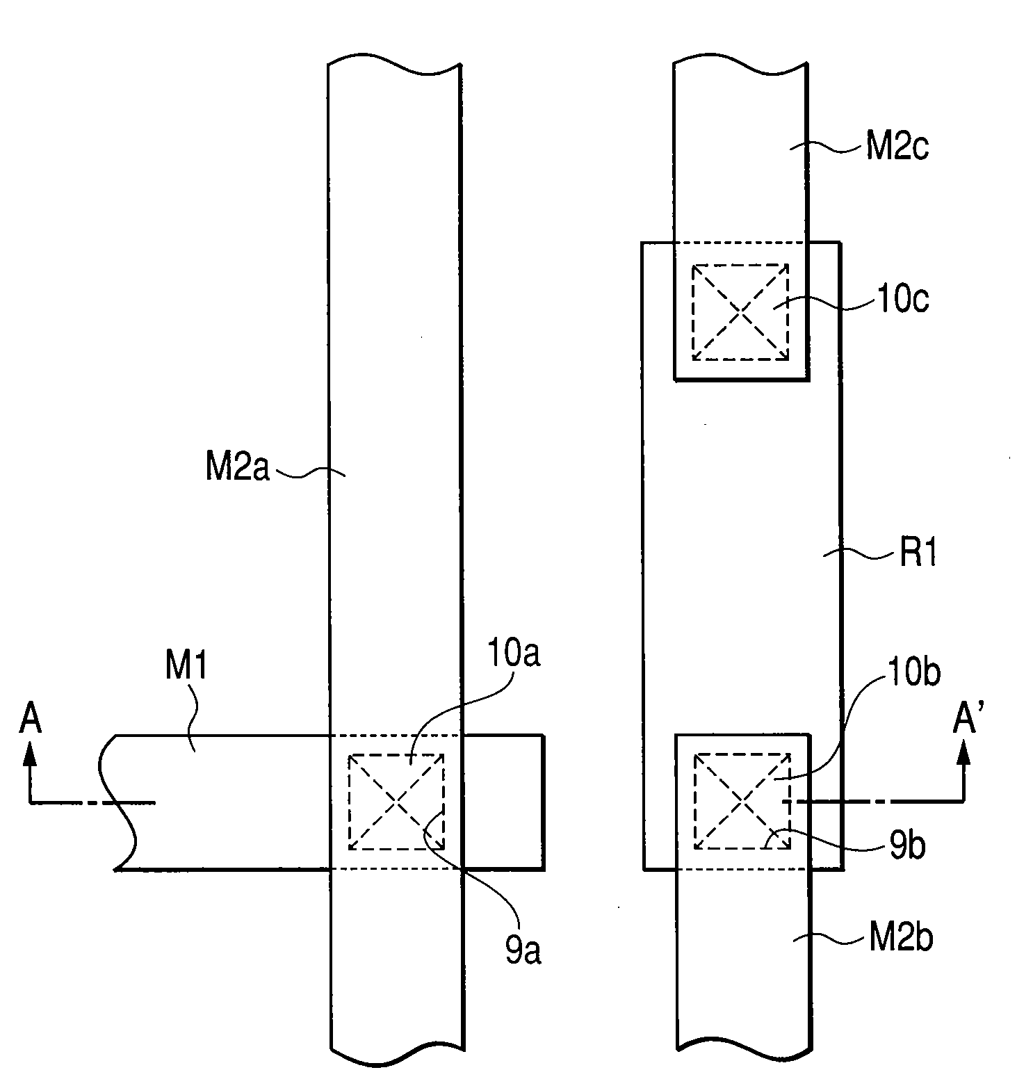
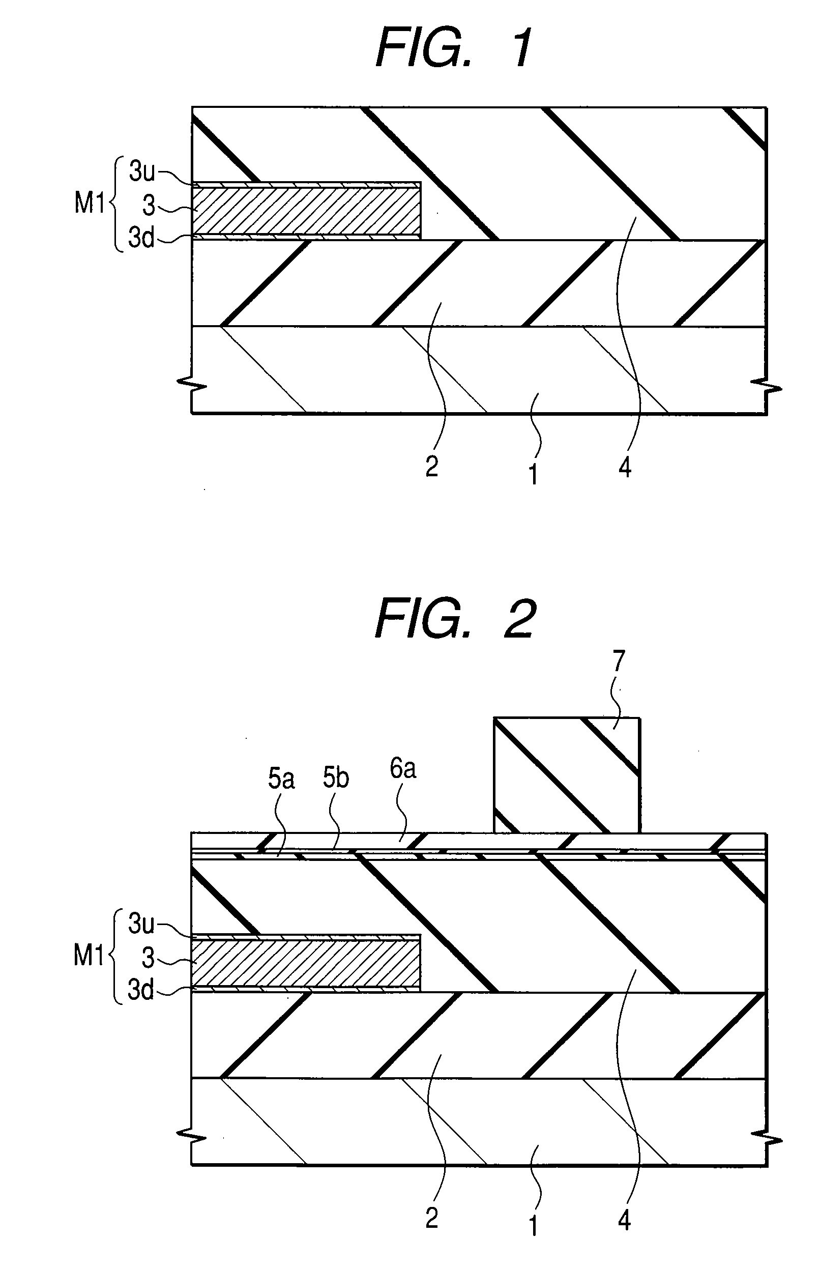
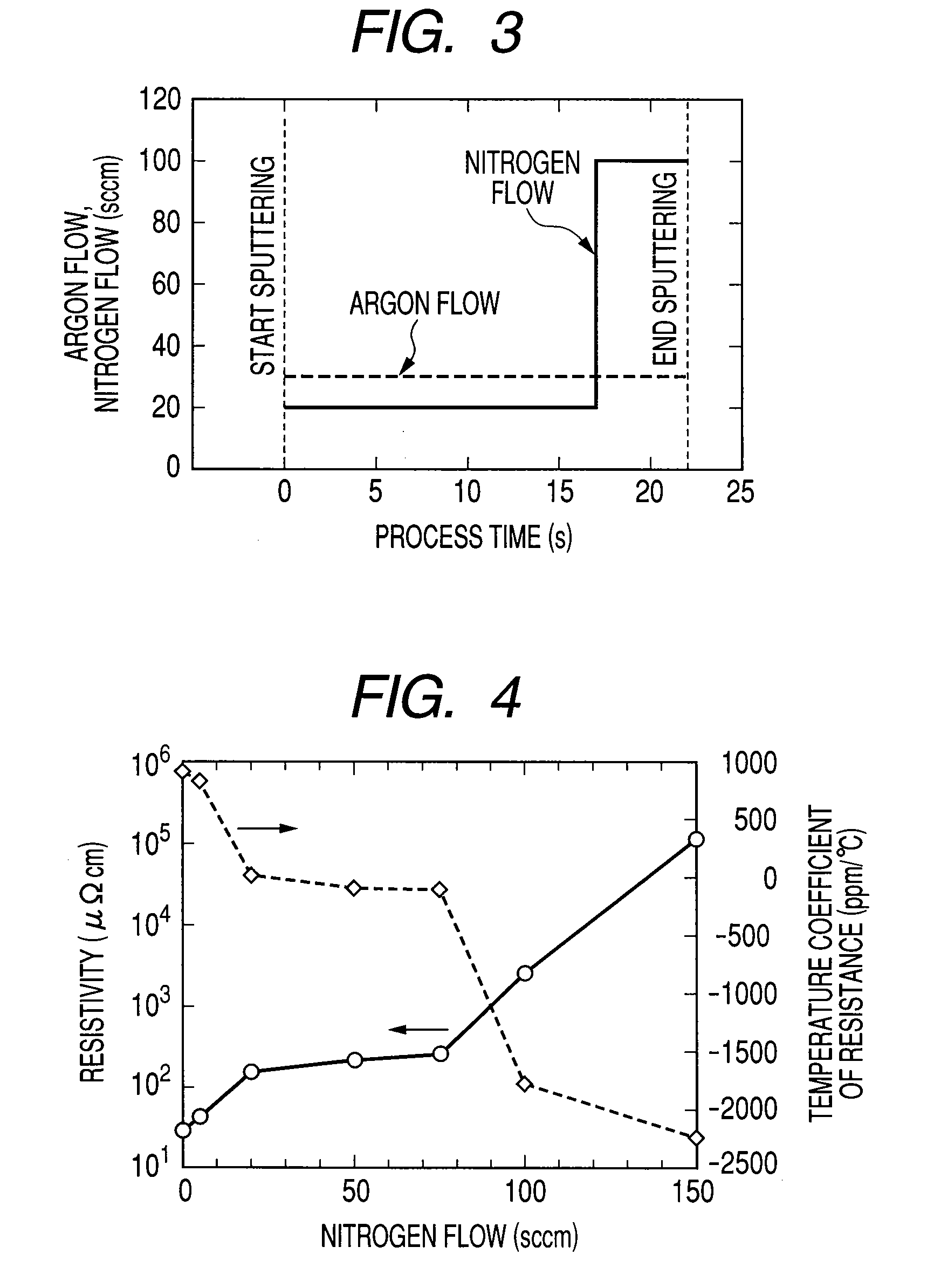
[0046]An example of a method of forming a resistor according to a first embodiment of the invention is to be described with reference to FIG. 1 to FIG. 11 in the order of steps. FIG. 1 and FIG. 2 are cross sectional views for a main portion showing a method of manufacturing a resistor, FIG. 3 is a graph showing a sputtering sequence upon forming a resistor layer, FIG. 4 is a graph showing the dependence of a resistivity or temperature coefficient of resistance on a nitrogen gas flow rate of a tantalum nitride film formed by a reactive DC sputtering method, FIG. 5 to FIG. 8 are cross sectional views for a main portion showing a manufacturing method of the resistor, FIG. 9 is a planar layout view of the resistor, FIG. 10 is a graph showing a relation between the resistance change ratio and the thickness of the second resistor layer of the resistor, and FIG. 11 is an analysis view showing X-diffraction pattern of a tantalum nitride film formed by sputtering method while varying a nitro...

second embodiment

[0074]A resistor R2 according to a second embodiment of the invention is constituted with a tantalum nitride film in the same manner as the resistor R1 according to the first embodiment described above. However, the resistor R2 is different from the resistor R1 of the first embodiment described above for the concentration of nitrogen contained in the tantalum nitride film and this is a resistor in which the concentration of nitrogen in the upper region situated on the side opposite to the substrate and in the lower region on the side of the substrate is higher than the concentration of nitrogen in the middle region. The resistor R2 according to the second embodiment is to be described with reference to the cross sectional view for the main portion of the resistor R2 shown in FIG. 12. Since the structure and the manufacturing process other than those for the tantalum nitride film constituting the resistor R2 are identical with those of the first embodiment described above, descriptio...

third embodiment

[0078]The resistor R3 according to the third embodiment of the invention is formed of a tantalum nitride film in the same manner as the resistor R1 according to the first embodiment described above. However, in the resistor R3, the fabrication method for the first and the second resistor layers 5a, 5b deposited above the second interlayer dielectric film 4 is different from the fabrication method for the first embodiment described above, and the first and the second resistor layers 5a, 5b are fabricated by using a first resist pattern 7 as a mask not using the first hard mask 6. A method of manufacturing the resistor R3 according to the third embodiment is to be described with reference to the cross sectional view for a main portion of the resister R3 shown in FIG. 13. Since the structure and the manufacturing process other than those for the tantalum nitride film constituting the resistor R3 are identical with those in the first embodiment described above, explanations therefor are...


PUM

PropertyMeasurementUnit
Thicknessaaaaaaaaaa
Fractionaaaaaaaaaa
Concentrationaaaaaaaaaa

Abstract

A resistor R1 formed by forming a first resistor layer 5a of 20 nm thickness including a tantalum nitride film at a concentration of nitrogen of less than 30 at % and a second resistor layer of 5 nm thickness including a tantalum nitride film at a concentration of nitrogen of 30 at % or more successively by a reactive DC sputtering method using tantalum as a sputtering target material and using a gas mixture of argon and nitrogen as a sputtering gas, and then fabricating the first and the second resistor layers, in which the resistance change ratio of the resistor can be suppressed to less than 1% even when a thermal load is applied in the interconnection step, by the provision of the upper region at a concentration of nitrogen of 30 at % or more.

Description

CLAIM OF PRIORITY[0001]The present application claims priority from Japanese patent application JP 2007-184614 filed on Jul. 13, 2007, the content of which is hereby incorporated by reference into this application.FIELD OF THE INVENTION[0002]The present invention relates to a semiconductor device and a technique for manufacturing the same and more particularly to a technique effective for application to a semiconductor device having a resistor composed of a metal film and a method of manufacturing the same.BACKGROUND OF THE INVENTION[0003]In a semiconductor device handling analog signals, passive elements such as a capacitor, a resistor, and an inductor are important constituent elements for integrated circuits. Since such passive elements are difficult to be fabricated into a semiconductor chip, they have been mounted as external parts on a packaging substrate. However, since requirement for increasing the operation speed of a system and space saving have become increased in recent...

Claims


Application Information

Patent Timeline
IPC IPC(8): H01C17/06H01C1/02
CPCH01C7/006H01C17/12H01L23/5228H01L27/016Y10T29/49099H01L2924/0002H01L28/20H01L2924/00
Inventor TAKEDA, KENICHIFUJIWARA, TSUYOSHIIMAI, TOSHINORI
Owner HITACHI LTD
Why Eureka
Try Eureka