Eureka AIR delivers breakthrough ideas for toughest innovation challenges, trusted by R&D personnel around the world.

IrOx nanowire protein sensor

a protein sensor and nanowire technology, applied in the field of integrated circuit fabrication, can solve the problems of insufficient single protein marker testing, material not suitable for multiplexing detection, and unreachable goal, and achieve the effect of reducing background noise effects and improving signal-to-noise ratio

Inactive Publication Date: 2009-01-15
SHARP LAB OF AMERICA INC
View PDF3 Cites 43 Cited by
  • Summary
  • Abstract
  • Description
  • Claims
  • Application Information

AI Technical Summary

Benefits of technology

[0013]This disclosure presents integrated nanowire arrays in which distinct nanowire surfaces can be integrated with distinct receptors / antibodies, to function as individual components of device elements. The detection technique is such that the variation in the electrical conductivity associated with the binding of specific proteins onto selectively functionalized nanowire arrays can be measured. The result is an electrochemical signature that is unique to a specific antibody or protein / antigen pair. Non-specific bindings can be eliminated by such a technique, thus reducing background noise effects considerably and improving the signal to noise ratio. The individual device elements, due to their specific functionalization, are able to detect specific proteins. Hence, a large array of proteins can be detected in a matrix format within a few minutes i.e., in near real time as opposed to conventional detection methods that range from a few hours to a few days. The quantity of test sample required for such detection process is in the order of microliters, as compared to milliliters in the conventional methods.
[0014]Iridium oxide nanowires are used as the active elements in the detection process. These nanowires are biocompatible, and amenable to the addition of multifunctionality suitable for multiplexed detection. The large surface area afforded by these nanowires enables a reduction in the device footprint by increasing the active area for detection. Comparing to a planar IrO2 electrode, IrO2 nanowires have an improved surface-to-volume ratio, resulting in a high selectivity, high sensitivity larger linear dynamic range of detection, and rapid response time.
[0015]As noted above, iridium oxide has very good conductivity and charge storing capacity. As such, it can be used to detect even a very small change in surface charge. High selectivity can be achieved by incorporating protein receptors (antibodies) on the nanowires, which bind only to specific proteins. This binding induces a change in surface charge, on the nanowire surface. This change in surface charge is due to the modification of the surface charge of the proteins as a result of the binding, which can be efficiently detected. This technique is extremely sensitive to these surface charge variations, enabling the detection of very small concentrations of proteins.

Problems solved by technology

For these complex diseases, the heterogeneity of the disease makes tests of single protein markers inadequate.
This goal has not yet been achieved by any of the existing detection methods that include the use of micro cantilevers, surface plasmon resonance, enzyme linked immunosorbant assays (ELISA). and carbon nanotube based sensors.
However, these materials are not suitable for multiplexed detection due to the complexity associated with the device fabrication and issues with repeatability.
However, a key issue to be resolved is the fabrication of an electrode array that can conform to concave shapes.
Another limitation associated with micromachining technology is size, as the individually machined electrodes cannot be made to a nano-size resolution.
Even if a template of nano-sized structures could be micro-machined, plating an array of nanostructures, with a noble metal for example, in a sufficiently high aspect ratio is a big challenge.
However, it is difficult to form single-crystal IrO2 films using conventional PVD or electrode plating methods.
IrO2 nanostructures can be formed using a solution method, but these structures have a low mechanical strength and poor crystal quality.
Vapor phase transport methods can also be used to form IrO2 nanostructures, but this process requires high substrate temperature, and it is not suitable for use with glass and polyimide substrates.

Method used


Image

  • IrOx nanowire protein sensor
  • IrOx nanowire protein sensor
  • IrOx nanowire protein sensor

Examples


Embodiment Construction

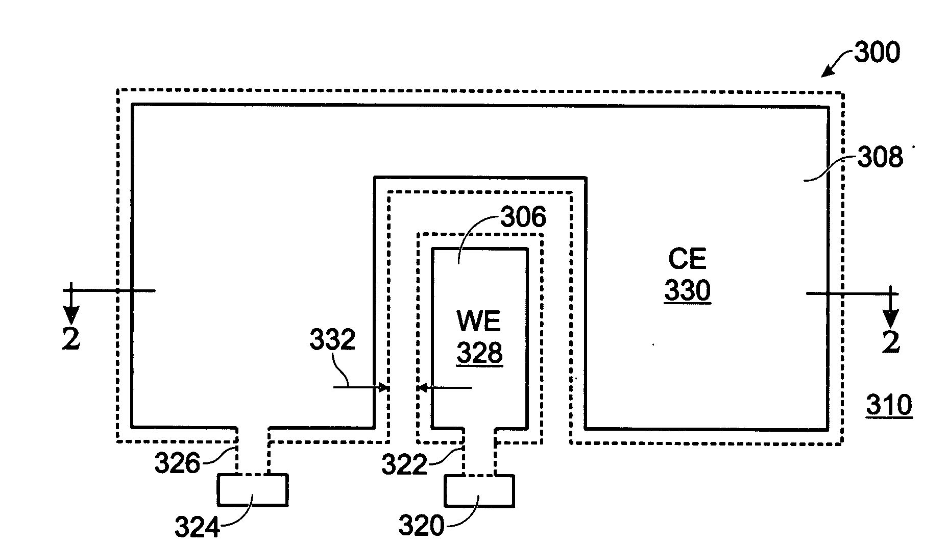
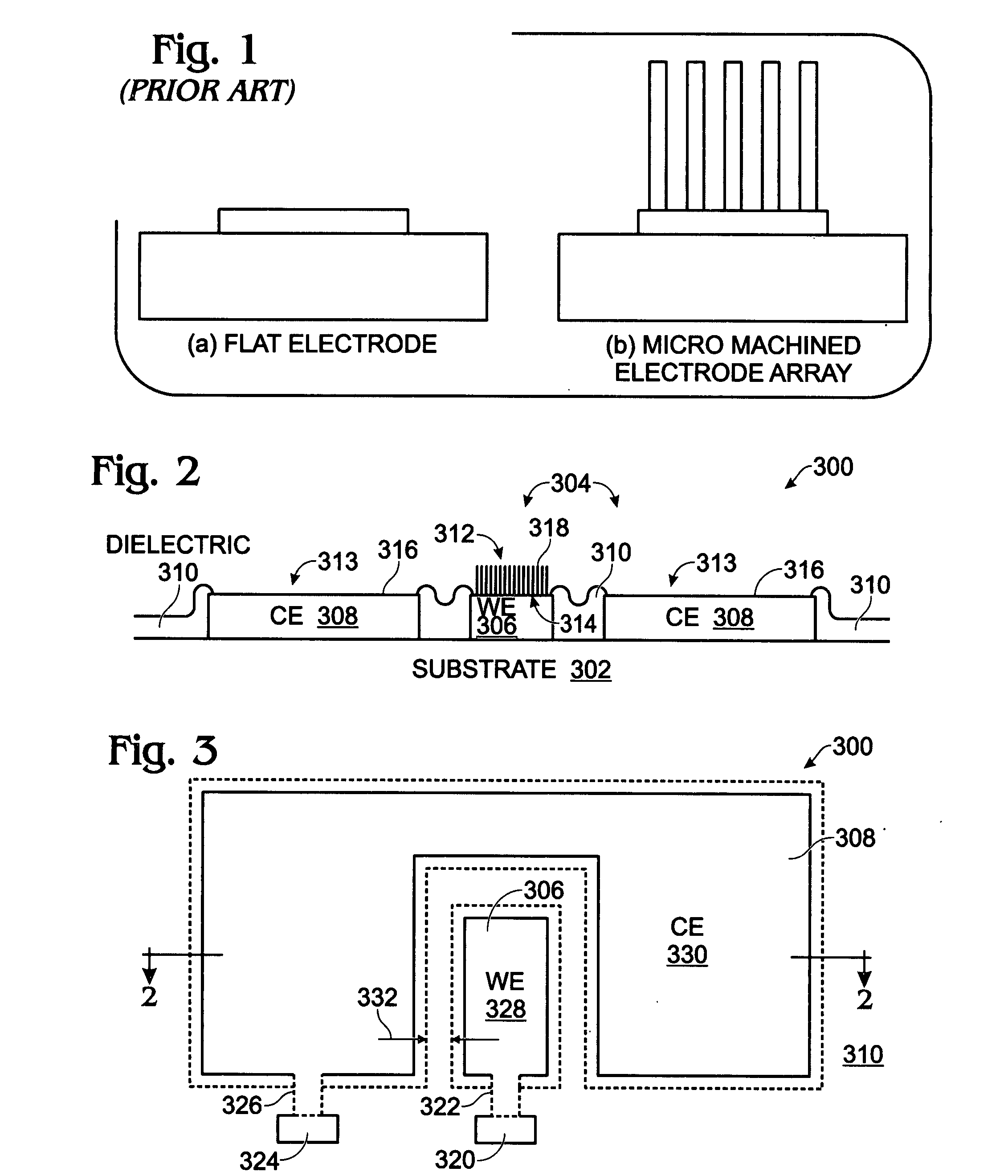
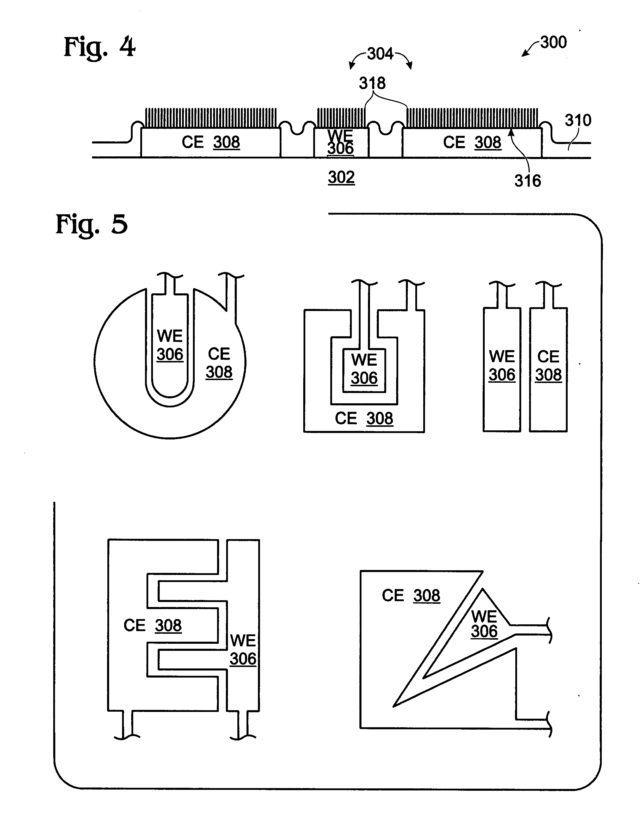
[0038]FIGS. 2 and 3 are partial cross-sectional and plan views, respectively of an iridium oxide (IrOx) nanowire protein sensor array. The sensor array 300 comprises a substrate 302 and a plurality of electrode pairs 304. For simplicity, FIGS. 2 and 3 show a single pair. Each electrode pair, as represented by pair 304, includes a working electrode (WE) 306 overlying the substrate 302 and a counter electrode (CE) 308 overlying the substrate 302. A dielectric layer 310 overlies the working and counter electrodes 306 / 308. Contact holes 312 and 313 are formed in the dielectric layer 310, exposing regions 314 and 316, respectively, of the working electrode 306 and the counter electrode 308. IrOx (0318 are grown from exposed region 314 of the working electrode 306. In some aspects, single-crystal IrO2 nanowires are grown. The electrode pair 304 may further include a coating of a material such as antibody linker molecules, antibodies, protein blocker agents, or combinations of the above-me...


PUM

PropertyMeasurementUnit
Temperatureaaaaaaaaaa
Lengthaaaaaaaaaa
Angleaaaaaaaaaa

Abstract

An iridium oxide (IrOx) nanowire protein sensor and associated fabrication method are presented. The method provides a substrate and forms overlying working and counter electrodes. A dielectric layer is deposited over the working and counter electrodes and contact holes are formed in the dielectric layer, exposing regions of the working and counter electrodes. IrOx nanowires (where 0≦X≦2) are grown from exposed regions of the working electrode. In one aspect, the IrOx nanowires are additionally grown on the dielectric, and subsequently etched from the dielectric. In another aspect, IrOx nanowires are grown from exposed regions of the counter electrode.

Description

BACKGROUND OF THE INVENTION[0001]1. Field of the Invention[0002]This invention generally relates to integrated circuit (IC) fabrication and, more particularly, to a fine resolution protein sensor fabricated with iridium oxide nanowire electrodes.[0003]2. Description of the Related Art[0004]The current industry standard for protein detection is fluorescent-based detection. Other detection means include: (1) Amperometry, (2) Potentiometry, and (3) Conductance. Table 1 highlights the advantages and shortcomings of these techniques for protein sensing.TABLE 1Comparison of Protein Sensing TechnologiesFluorescencePotentiometry andCapacitance MethodmethodAmperometryHigh sensitivity ofLow Sensitivity ofLow Sensitivity ofdetection:detection:detection:femto-molar rangenano to pico molarnano to pico molarRapid response time:Response time veryResponse time high:seconds to minuteshigh: Hours to daystens of minutes tohoursHigh Signal-to-NoiseLow Signal to NoiseLow Signal to NoiseRatio: Above 95%R...

Claims


Application Information

Patent Timeline
IPC IPC(8): B05D5/12C12M1/00
CPCG01N33/5438G01N27/4146
Inventor ZHANG, FENGYANREDDY, RAVI K.ULRICH, BRUCE D.PRASAD, SHALINIHSU, SHENG TENG
Owner SHARP LAB OF AMERICA INC
Why Eureka
Eureka Blog
Learn More