Structures of ordered arrays of semiconductors

a semiconductor and array technology, applied in the field of structure for the conversion of light into energy, can solve the problems of difficult to meet the requirements of the material of the absorber, and the situation is especially severe for the indirect band gap absorber, etc., to achieve low minority carrier diffusion length, high impurity density, and low density of defects

Inactive Publication Date: 2009-01-22
CALIFORNIA INST OF TECH
View PDF48 Cites 75 Cited by
  • Summary
  • Abstract
  • Description
  • Claims
  • Application Information

AI Technical Summary

Benefits of technology

[0008]Inexpensive candidate materials for use in photovoltaic applications generally have either a high level of impurities or a high density of defects, resulting in low minority-carrier diffusion lengths. The use of such low diffusion-length materials as the absorbing base in a conventional planar p-n junction solar-cell geometry results in devices having a carrier collection limited by minority-carrier diffusion in the base region. Increasing the thickness of the base in such a cell will therefore produce more light absorption but will not result in an increase in device efficiency. In the absence of sophisticated light-trapping schemes, materials with low diffusion lengths and low absorption coefficients therefore cannot be readily incorporated into planar solar-cell structures with high energy-conversion efficiency.

Problems solved by technology

This constraint imposes a cost floor on the absorber material by dictating the minimum required purity of the absorber phase.
The situation is especially severe for indirect band gap absorbers, such as Si which requires over 100 μm of thickness to absorb 90% of the energy in sunlight above the 1.12 eV band gap of Si.
Inexpensive candidate materials for use in photovoltaic applications generally have either a high level of impurities or a high density of defects, resulting in low minority-carrier diffusion lengths.
The use of such low diffusion-length materials as the absorbing base in a conventional planar p-n junction solar-cell geometry results in devices having a carrier collection limited by minority-carrier diffusion in the base region.
Increasing the thickness of the base in such a cell will therefore produce more light absorption but will not result in an increase in device efficiency.
In the absence of sophisticated light-trapping schemes, materials with low diffusion lengths and low absorption coefficients therefore cannot be readily incorporated into planar solar-cell structures with high energy-conversion efficiency.

Method used


Image

  • Structures of ordered arrays of semiconductors
  • Structures of ordered arrays of semiconductors
  • Structures of ordered arrays of semiconductors

Examples


example 1

Photoelectrochemical Cell Comprising Grown Semiconductor Structures

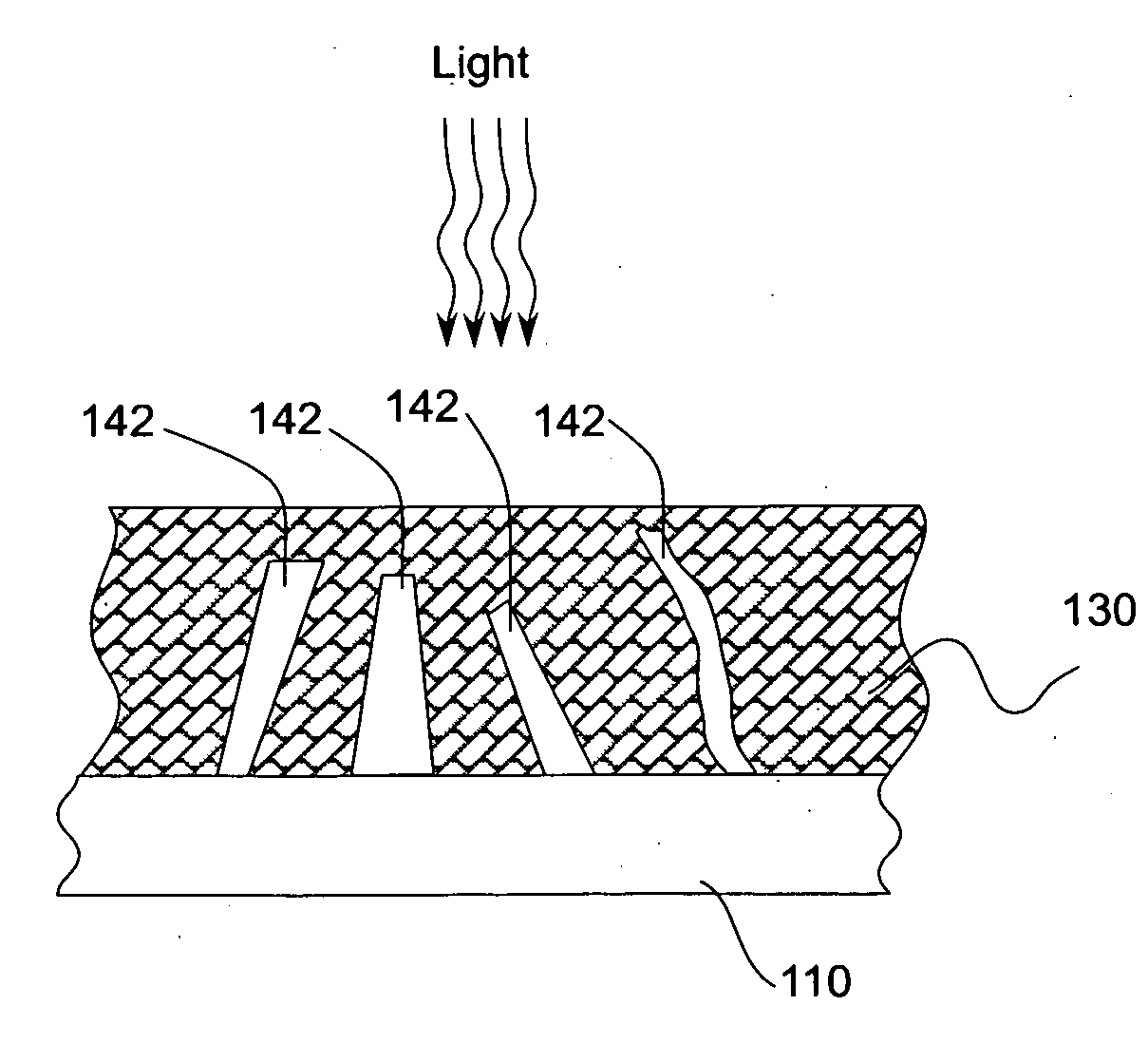
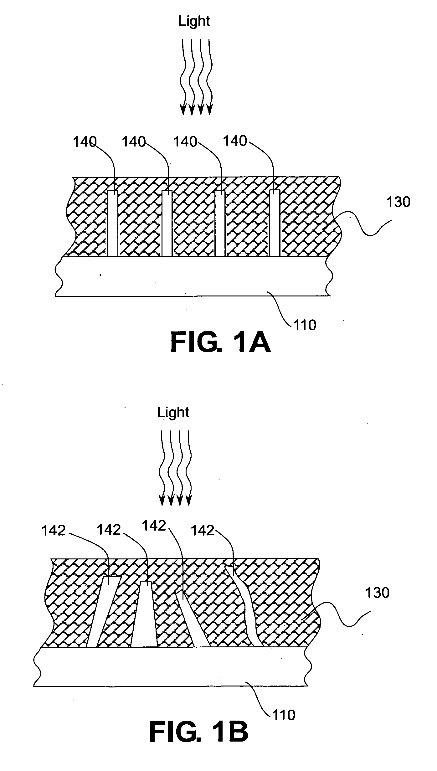
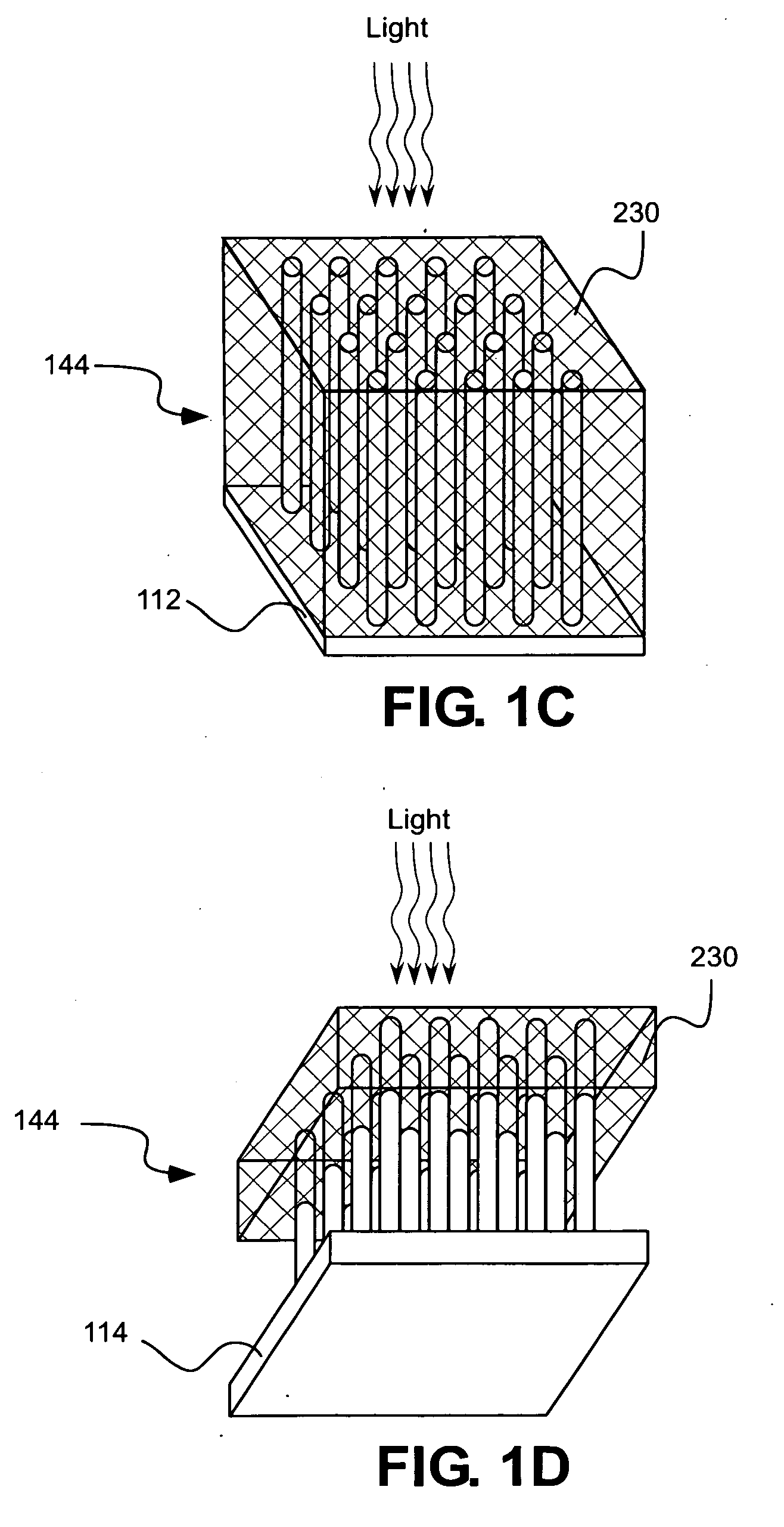
[0044]As described in additional detail below, vertically-aligned wire arrays may be used for solar energy conversion where the wires in the arrays provide primary light absorption and charge carrier separation. Preferably, wires in the vertically-aligned wire arrays are formed with relatively high aspect ratios, that is, wires in the wire arrays are long in the direction of received light, but have relatively small radii to facilitate efficient radial collection of carriers. These radii can be small even for relatively impure absorber materials. Solar cell devices according to an embodiment of the present invention have relatively large area arrays of vertically aligned wires, means to make electrical junctions to such wire arrays and means to make electrical contacts to the backsides of these devices. In one embodiment, solar energy conversion is obtained by using wires as the primary light absorption and charge ca...

example 2

Photoelectrochemical Cell Comprising Deposited Semiconductor Structures

[0066]Another embodiment of the present invention comprises a photoelectrochemical cell having radial rod array junction photoelectrodes prepared by electrodeposition of Cd(Se, Te) and is described below. The II-VI semiconductors CdSe and CdTe are both direct gap, highly absorbing materials having band gaps (1.7 eV for CdSe and 1.4 eV for CdTe) well-matched to the solar spectrum. The materials can both be deposited by a number of techniques. Electrodeposition of CdTe and CdSe is well established, and the photovoltaic or photoelectrochemical cell performance of the electrodeposited forms of these materials are usually limited by low minority-carrier collection diffusion lengths in the absorber phase.

[0067]Embodiments of the present invention may use several methods for the fabrication of entire arrays of vertically aligned semiconductor nanorods. When a deposition technique that does not induce one-dimensional gro...

example 3

Photoelectrochemical Cell Comprising Etched Semiconductor Structures

[0086]Another embodiment of the present invention comprises a photoelectrochemical cell having silicon pillars produced by etching a planar substrate. The silicon etched pillars may be fabricated using a low temperature Reactive Ion Etching (RIE) process. Such a process may be performed at nearly liquid nitrogen temperatures and can produce very deep etched structures. The planar substrate may be etched using photoresist as the masking medium. FIGS. 17A-17G show SEM images of pillars prepared by using an etch process. The photomask used to pattern the resist had areas containing arrays of 5, 10, 20, and 50 um diameter spots spaced in a hexagonal close packed array so that the same total filling fraction of pillars would result in each case. FIG. 17A shows an array of 50 μm diameter pillars and FIG. 17B shows a single 50 μm diameter pillar. FIG. 17C shows 20 μm diameter pillars. FIG. 17D shows 10 μm diameter pillars ...


PUM


Abstract

A device having arrays of semiconductor structures with dimensions, ordering and orientations to provide for light absorption and charge carrier separation. The semiconductor structures are formed with relatively high aspect ratios, that is, the structures are long in the direction of received light, but have relatively small radii to facilitate efficient radial collection of carriers.

Description

CROSS-REFERENCE TO RELATED APPLICATIONS[0001]The present application is related to and claims the benefit of the following copending and commonly assigned U.S. Patent Applications: U.S. Patent Application No. 60 / 961,170, titled “Fabrication of Wire Array Samples and Controls,” filed on Jul. 19, 2007; U.S. Patent Application No. 60 / 961,169, titled “Growth of Vertically Aligned Si Wire Arrays Over Large Areas (>1 cm2) with Au and Cu Catalysts,” filed on Jul. 19, 2007; U.S. Patent Application No. 60 / 961,172, titled “High Aspect Ratio Silicon Wire Array Photoelectrochemical Cells,” filed on Jul. 19, 2007; U.S. Patent Application No. 60 / 966,432, titled Polymer-embedded semiconductor rod arrays,” filed on Aug. 28, 2007 and U.S. Patent Application No. 61 / 127,437, titled “Regrowth of Silicon Rod Arrays,” filed on May 13, 2008, the entire contents of all of these applications are incorporated herein by reference.[0002]The present application is also related to the following copending and ...

Claims


Application Information

Patent Timeline
Patent Type & Authority Applications(United States)
IPC IPC(8): H01L31/00
CPCH01G9/2054Y02E10/542H01L31/101H01L31/0352
Inventor ATWATER, HARRY A.KAYES, BRENDAN M.LEWIS, NATHAN S.MAIOLO, III, JAMES R.SPURGEON, JOSHUA M.
Owner CALIFORNIA INST OF TECH
Why Eureka
Try Eureka