Manufacturing method of display device
a manufacturing method and display device technology, applied in non-linear optics, instruments, coatings, etc., can solve the problems of poor productivity of microcrystalline silicon tft, inability to employ such a low deposition rate, and inability to manufacture a display device, so as to reduce the deposition rate and ensure the effect of manufacturing efficiency
- Summary
- Abstract
- Description
- Claims
- Application Information
AI Technical Summary
Benefits of technology
Problems solved by technology
Method used
Image

Examples
embodiment modes
[0044]Embodiment modes of the present invention will be described below with reference to the accompanying drawings. Note that the present invention is not limited to the description below, and it is easily understood by those skilled in the art that modes and details can be modified in various ways without departing from the purpose and the scope of the present invention. Accordingly, the present invention should not be interpreted as being limited to the description of the embodiment modes below. Note that like portions in the drawings may be denoted by the like reference numerals in structures of the present invention.
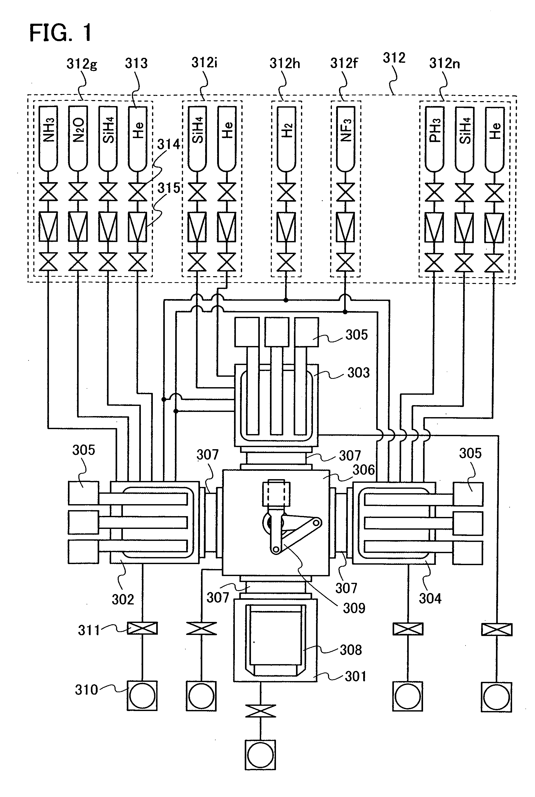
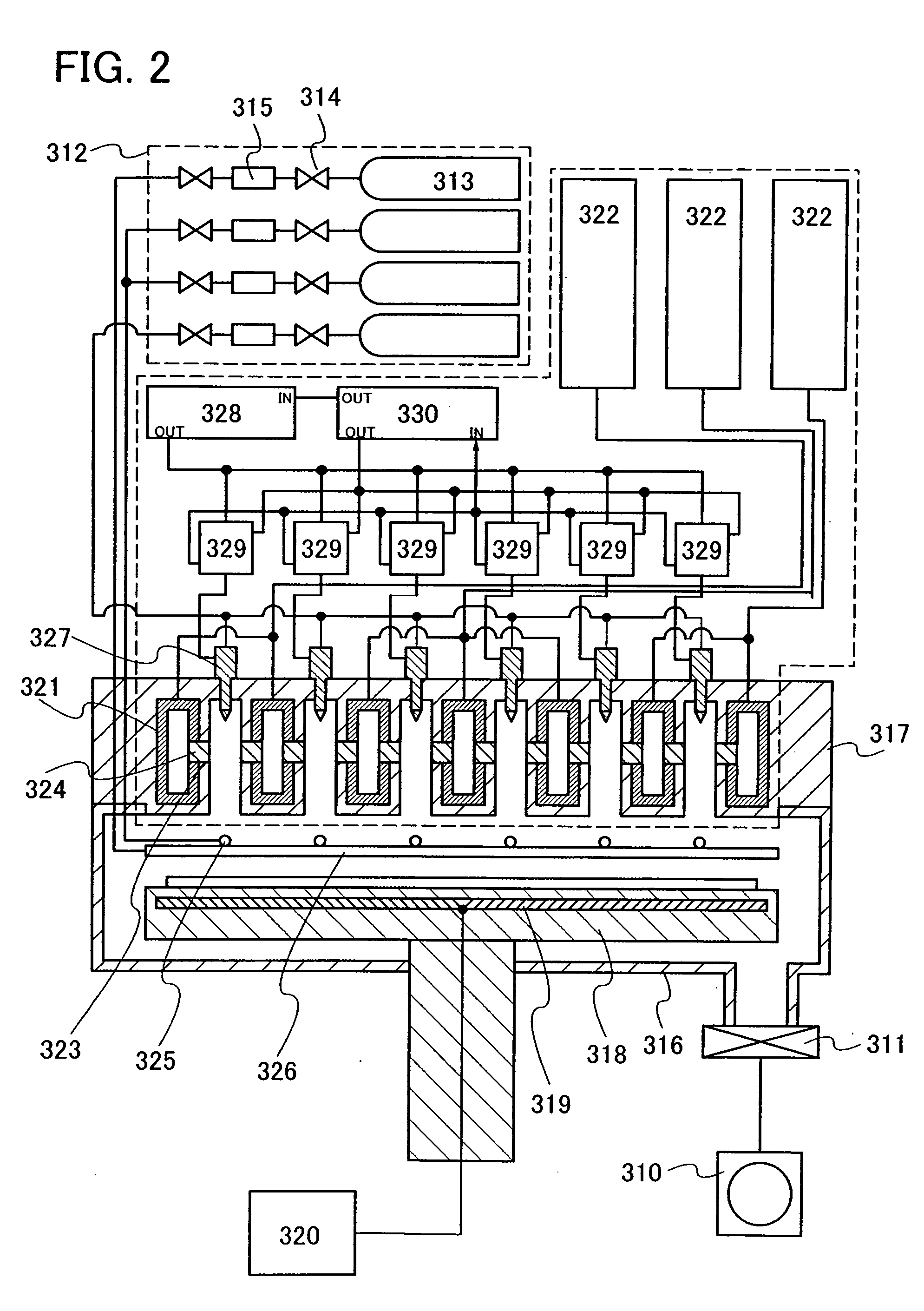
(Structural Example of Multi-Chamber Microwave Plasma CVD Apparatus)
[0045]A microcrystalline semiconductor layer is formed by a plasma CVD method. In this embodiment mode, an atmospheric pressure or a sub-atmospheric pressure is applied as a film formation condition of a microcrystalline semiconductor layer. The range of 1×10² Pa or more and 1×10⁵ Pa or less (1 Torr...
embodiment mode 1
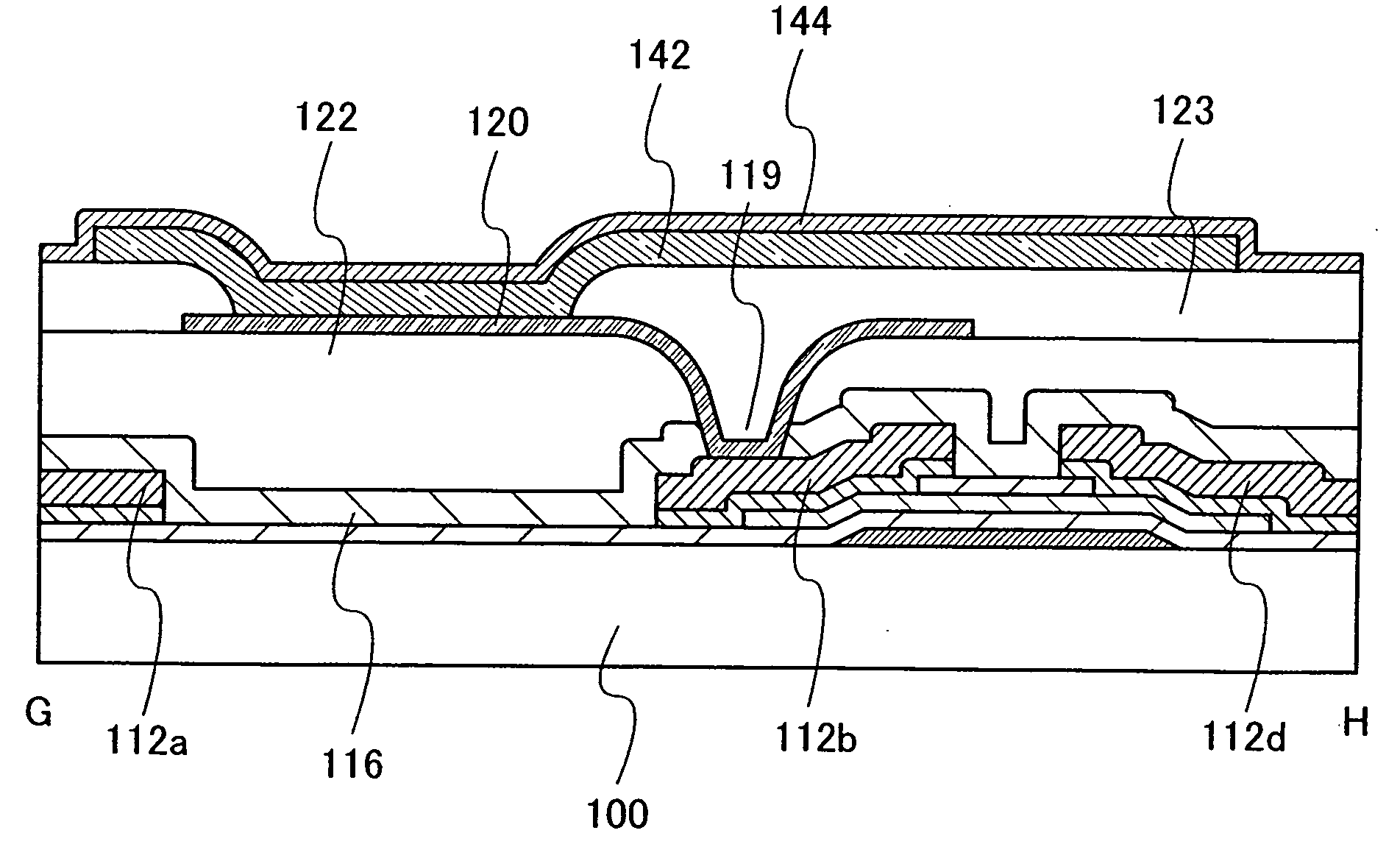
[0070]A manufacturing process of a display device including a TFT having a channel formed of a microcrystalline semiconductor layer will be described with reference to the drawings. FIGS. 8, 9, 10, and 11 are each a plan view of a pixel, and cross-sectional views taken along line A-B in FIGS. 8, 9, 10, and 11 are shown in FIGS. 12, 13, 14, 15, and 16, respectively. The following description is made with reference to these plan views and cross-sectional views as appropriate.
(1) Formation of Gate Electrode and Capacitor Electrode
[0071]As an element substrate 100 where a TFT is manufactured, a flat substrate having an insulating surface such as a glass substrate is applied. A gate electrode layer 102 and a capacitor electrode layer 104 are formed over the element substrate 100 (FIGS. 8 and 12).
[0072]The gate electrode layer 102 and the capacitor electrode layer 104 are formed of a metal material. As a metal material, aluminum, chromium, titanium, tantalum, molybdenum, copper, or the li...
embodiment mode 2
[0091]This embodiment mode will exemplify pixels of a liquid crystal panel of a VA (vertical alignment)-mode liquid crystal, which has a so-called multi-domain design where a pixel is divided into some regions (sub-pixels). FIG. 17 shows a plan view of the pixel, and FIG. 18 shows a cross-sectional view taken along line C-D in FIG. 17.
[0092]The structure of an element substrate 100, a gate electrode layer 102, a capacitor electrode layer 104, a gate insulating layer 106, a microcrystalline semiconductor layer 108, an impurity semiconductor layer 110, wiring layers 112a and 112b, and a capacitor electrode layer 112c is the same as the structure in Embodiment Mode 1. An interlayer insulating layer 122 is formed over a protective insulating layer 116, and further a contact hole 117 which penetrates the interlayer insulating layer 122 and the protective insulating layer 116 is formed. The interlayer insulating layer 122 is formed of an inorganic insulating material such as silicon oxide...
PUM
| Property | Measurement | Unit |
|---|---|---|
| pressure | aaaaa | aaaaa |
| pressure | aaaaa | aaaaa |
| electron density | aaaaa | aaaaa |
Abstract
Description
Claims
Application Information
 - R&D
- Intellectual Property
- Life Sciences
- Materials
- Tech Scout
- Unparalleled Data Quality
- Higher Quality Content
- 60% Fewer Hallucinations
Browse by: Latest US Patents, China's latest patents, Technical Efficacy Thesaurus, Application Domain, Technology Topic, Popular Technical Reports.
© 2025 PatSnap. All rights reserved.Legal|Privacy policy|Modern Slavery Act Transparency Statement|Sitemap|About US| Contact US: help@patsnap.com