

Functional films formed by highly oriented deposition of nanowires
- Summary
- Abstract
- Description
- Claims
- Application Information
AI Technical Summary
Benefits of technology
Problems solved by technology
Method used
Image

Examples
example 1
Synthesis of Silver Nanowires
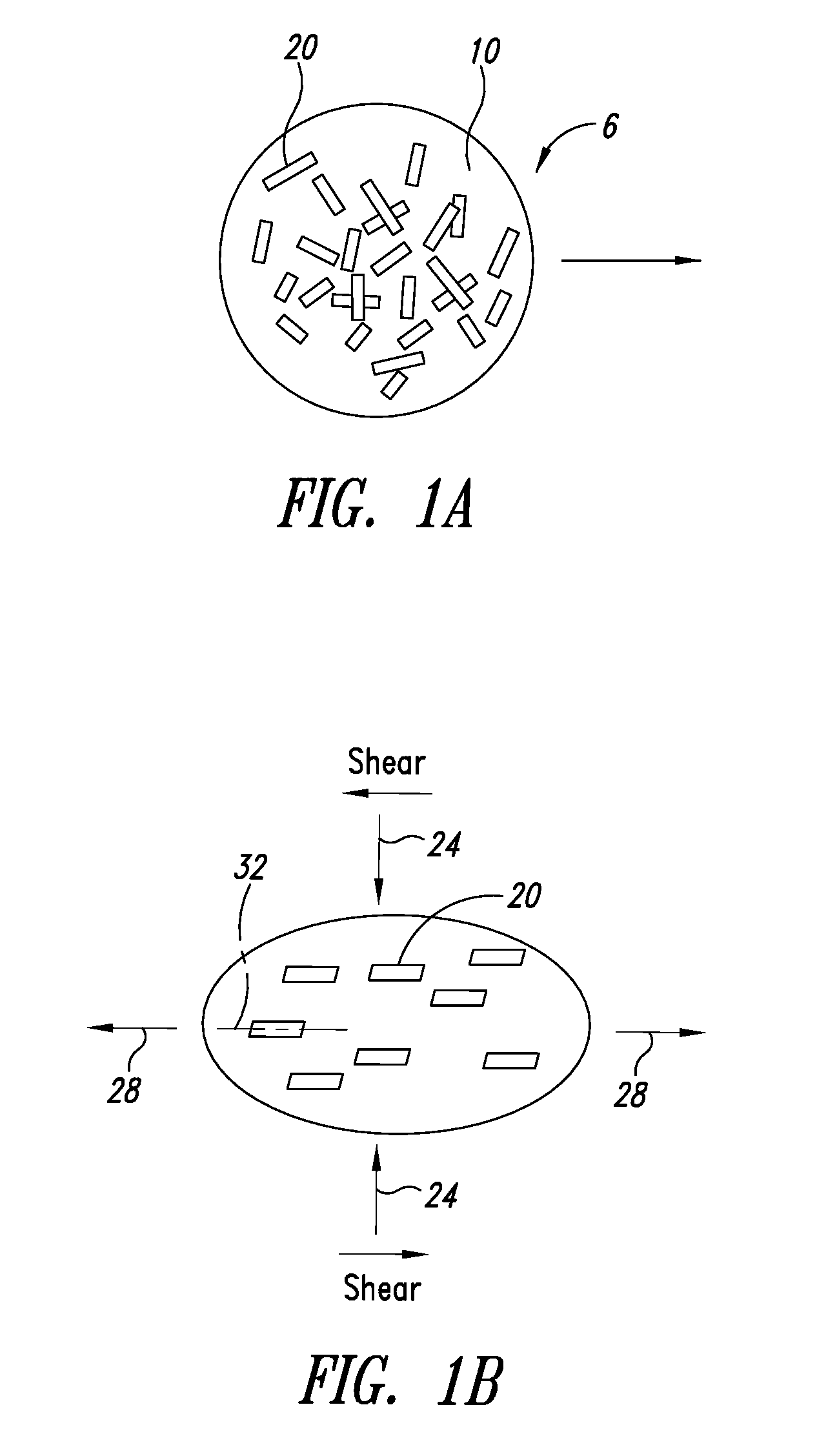
[0125]Silver nanowires were synthesized by a reduction of silver nitrate dissolved in ethylene glycol in the presence of poly(vinyl pyrrolidone) (PVP). The method was described in, e.g. Y. Sun, B. Gates, B. Mayers, & Y. Xia, “Crystalline silver nanowires by soft solution processing”, Nanolett, (2002), 2(2) 165-168. Uniform silver nanowires can be selectively isolated by centrifugation or other known methods.
[0126]Alternatively, uniform silver nanowires can be synthesized directly by the addition of a suitable ionic additive (e.g., tetrabutylammonium chloride) to the above reaction mixture. The silver nanowires thus produced can be used directly without a separate step of size-selection. This synthesis is described in more detail in U.S. Provisional Application No. 60 / 815,627, in the name of Cambrios Technologies Corporation, the assignee of the present application, which application is incorporated herein in it entirety.
[0127]In the following examples, s...
example 2
Flow-Directed Alignment of Silver Nanowires
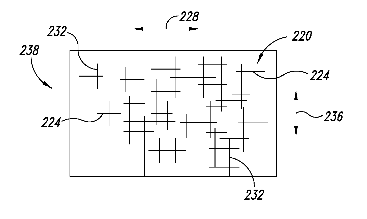
[0128]An Autoflex EBG5 polyethylene terephthalate (PET) film 5 mm thick was used as a substrate. The surface area was 10×13 cm. The PET substrate was incubated with 0.1 mg / ml poly-L-lysine (MW 500-2000) for an hour. An even layer of poly-L-lysine was coated on the PET substrate. The coating slightly reduced the light transmission of PET (about 92%). The coated PET substrate was then placed on a pivoting shaker.
[0129]Thereafter, a dispersion of silver nanowires in a solvent (e.g., low surface tension organic solvent) was deposited on the coated PET substrate. The pivoting shaker rocked for 2 hours, which induced a fluid flow in east-west directions (along the length of the substrate). The rocking motion was carried out at a tilting angle of no more than 18° from the pivoting axis. The substrate was then dried. As shown in FIG. 18A, substantially all of the nanowires are aligned in the east-west directions.
[0130]Subsequently, the PET substrat...
example 3
Preparation of a Transparent Conductor
[0132]The silver nanowire network formed on the PET substrate in Example 2 can be further processed by depositing a matrix material thereon. The matrix material can be prepared by mixing Polyurethane (PU) (Minwax Fast-Drying Polyurethane) in methyl ethyl ketone (MEK) to form a 1:4 (v / v) viscous solution. The matrix material was coated on the silver nanowire network by known methods in the art, for example, curtain coating. The matrix material can be cured for about 3 hours at room temperature, during which the solvent MEK evaporated and the matrix material hardened to form an optically clear matrix. Alternatively, the curing can be done in an oven, e.g., at a temperature of 50° C. for about 2 hours.
[0133]A transparent conductor having a conductive network of silver nanowires on the PET substrate (AgNW / PU / PET) can thus be formed. Typically, the presence of the matrix does not alter the electrical conductivity of the silver nanowire network. It ca...
PUM
| Property | Measurement | Unit |
|---|---|---|
| Fraction | aaaaa | aaaaa |
| Electrical resistance | aaaaa | aaaaa |
| Nanoscale particle size | aaaaa | aaaaa |
Abstract
Description
Claims
Application Information