

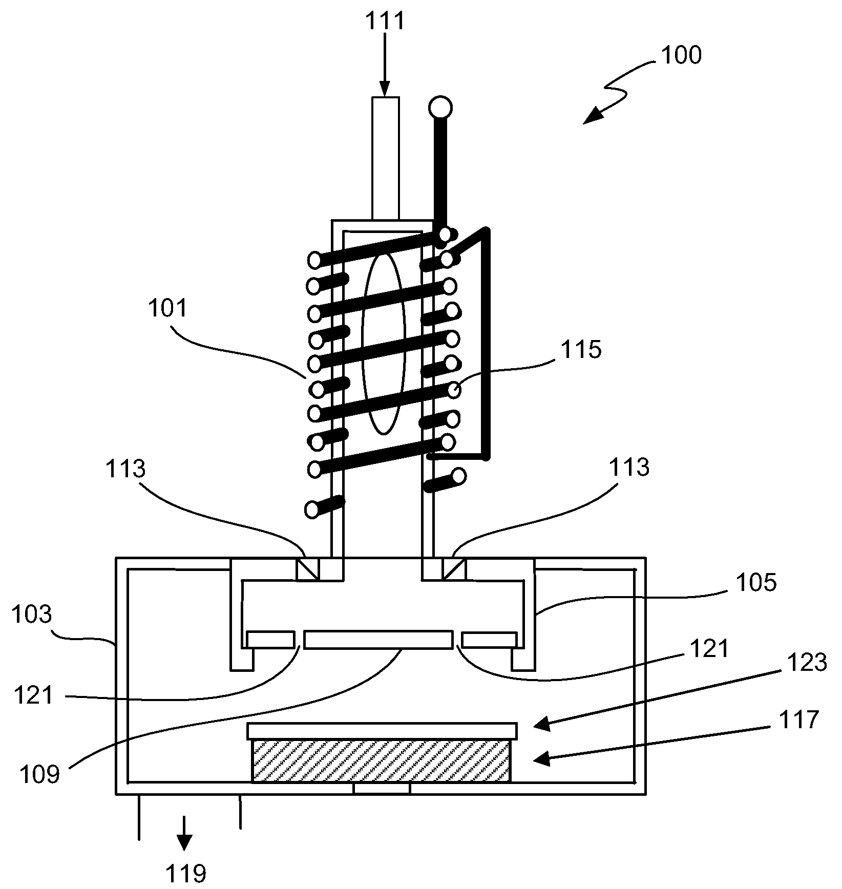
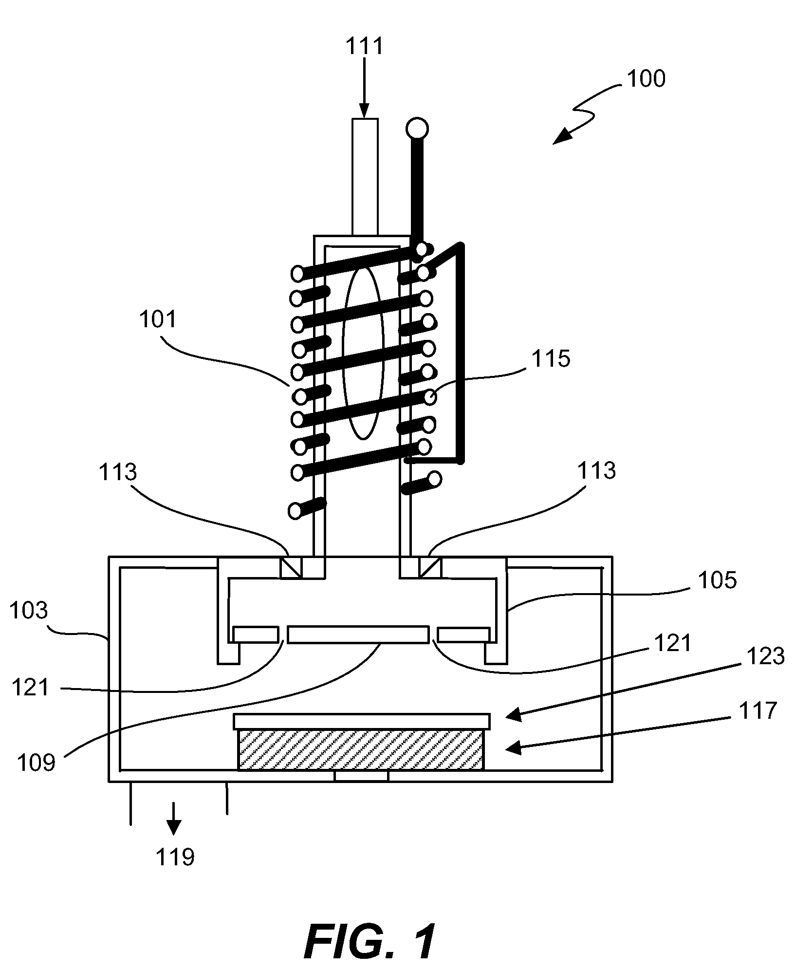
High dose implantation strip (HDIS) in h2 base chemistry
a technology of implantation strip and h2 base chemistry, which is applied in the direction of fluorine/hydrogenfluoride, chemistry apparatus and processes, fluorine, etc., can solve the problems of oxidation of implant atoms in the resist, sputtering during high-energy implants, and removing some of the underlying functional device structure, etc., to achieve low silicon loss
- Summary
- Abstract
- Description
- Claims
- Application Information
AI Technical Summary
Benefits of technology
Problems solved by technology
Method used
Image

Examples
example 1
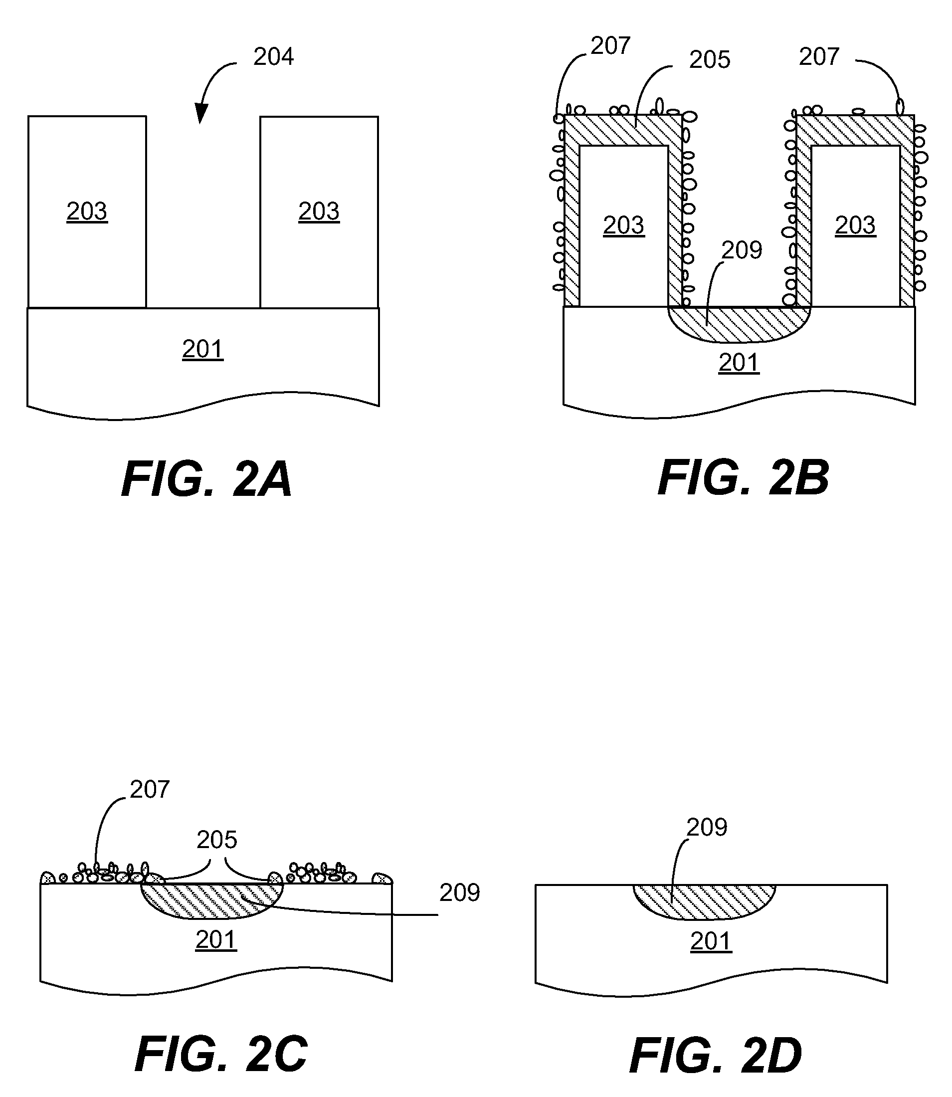
[0060]In this example, the impacts of carbon dioxide and carbon tetrafluoride on residue were investigated. 300 mm sized wafers were patterned with 45 nm structures and ion implanted with an LDD (lightly doped drain) in the P+ region. The resulting post high dose implant resist was about 2000 angstroms thick with a crust about 630 angstroms thick.
[0061]The wafers were stripped in a strip chamber having 5 plasma stations. The plasma was generated with RF power at 2000 Watts. The wafers were exposed to the plasma-activated reactive gas for about 20 seconds at each station for a total of 97 seconds. The wafer support temperature was 350 degrees Celsius. Chamber pressure was 900 mTorr. Hydrogen flow rate was 6 slm (standard liters per minute), and downstream argon flow rate was 14 slm. Carbon dioxide flow rate was varied between 0 and 150 sccm. Carbon tetrafluoride flow rate was varied between 20 and 40 sccm. Note that these flow rates are total flow rates for the entire chamber with 5 ...
example 2
[0064]In this example, the effects of carbon dioxide flow rate and carbon tetrafluoride flow rate on silicon loss were independently examined. Silicon loss for HDIS under the same process conditions as that of Example 1 was measured for carbon dioxide flow rates of 0, 50, 100, and 150 sccm while the carbon tetrafluoride flow rate was held constant at 40 sccm. The results are plotted in FIG. 5A. Silicon loss is lowest at carbon dioxide flow rate of 150 sccm and highest when no carbon dioxide is added. This result shows that some carbon dioxide in the plasma reduces silicon loss.
[0065]Silicon loss for HDIS under the same process conditions as that of Example 1 was also measured for carbon tetrafluoride flow rates of 0, 40, 60, 80, and 100 sccm while carbon dioxide flow rate was held constant at 150 sccm. The results are plotted in FIG. 5B. The silicon loss appears to peak at carbon tetrafluoride flow rates of 60 to 80 sccm.
[0066]These results show that silicon loss is affected by flow...
example 3
[0067]In another example, the effect of using different gas compositions at different stations was investigated relative to silicon loss and strip residue. The process conditions were the same as that of Example 1, except that the wafer support temperature is 250 degrees Celsius. In a first recipe, carbon tetrafluoride was employed in all stations at a total flow rate of 40 sccm. In a second recipe, carbon tetrafluoride was delivered only to RF stations 1 and 2 at a total flow rate of 20 sccm (10 sccm per station). Carbon dioxide flow rate was held constant at 150 sccm.
[0068]In both cases residue free substrates were obtained after HDIS process. The average silicon losses were 8.1 Å per cycle in the first recipe and 6.7 Å in the second recipe, a reduction of about 17%. A cycle is a complete pass through the tool, including processing at all stations. This result shows that a sequential stripping process using different gas compositions can reduce silicon loss while maintaining resid...
PUM
| Property | Measurement | Unit |
|---|---|---|
| temperature | aaaaa | aaaaa |
| pressure | aaaaa | aaaaa |
| pressure | aaaaa | aaaaa |
Abstract
Description
Claims
Application Information