Semiconductor device

a technology of semiconductor devices and semiconductors, applied in the field of semiconductor devices, can solve the problems of poor connection, operation defect, and problem of semiconductor device destruction, and achieve the effects of high yield, high reliability, and preventing creases

Inactive Publication Date: 2009-03-05
SEMICON ENERGY LAB CO LTD
View PDF24 Cites 34 Cited by
  • Summary
  • Abstract
  • Description
  • Claims
  • Application Information

AI Technical Summary

Benefits of technology

[0024]In the present invention, a structure body in which a fiber body of an organic compound or an inorganic compound is impregnated with an organic resin is used, whereby a highly reliable semiconductor device which is not easily damaged by local pressure from the outside can be manufactured with high yield.
[0025]In addition, since a planarized semiconductor device can be obtained according to the present invention, creases are prevented from occurring in the structure body in which the fiber body of the organic comp

Problems solved by technology

Further, in the case where a semiconductor device is manufactured by connecting an antenna provided for paper or a film medium to a chip, poor connection occurs when the size of the chip is small.
However, when the area of the chip is enlarged, a semiconductor device which is transferred to a plastic film or the like is cracked by local pressing force from the outside, resulting in an operation defect.
For example, when a character is written with a writing material on a plastic sheet or paper on a surface of a

Method used


Image

  • Semiconductor device
  • Semiconductor device
  • Semiconductor device

Examples


embodiment mode 1

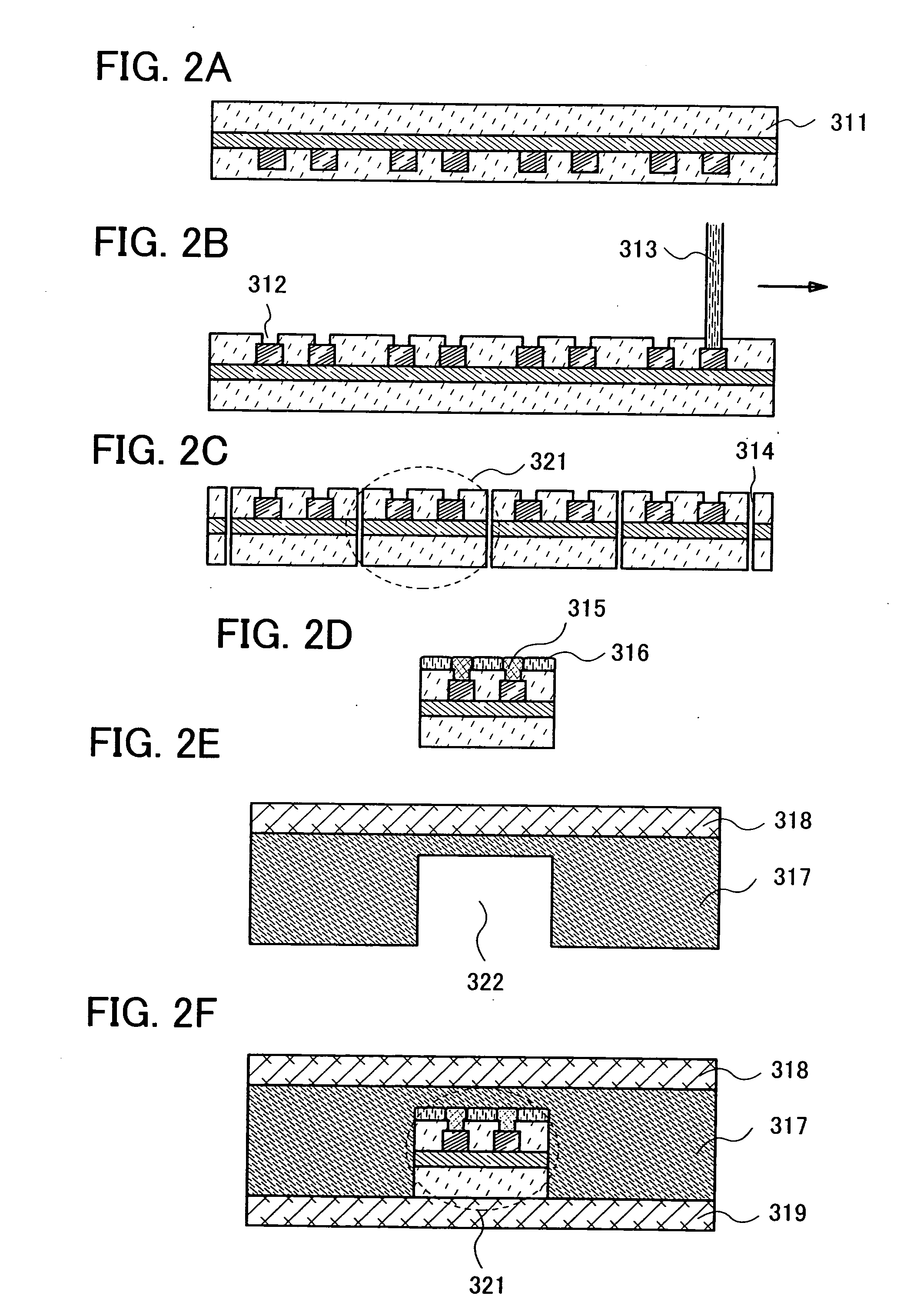
[0040]This embodiment is described with reference to FIGS. 1A to 1E, FIGS. 2A to 2F, FIGS. 3A to 3D, FIGS. 4A and 4B, FIGS. 5A to 5D, and FIG. 6.

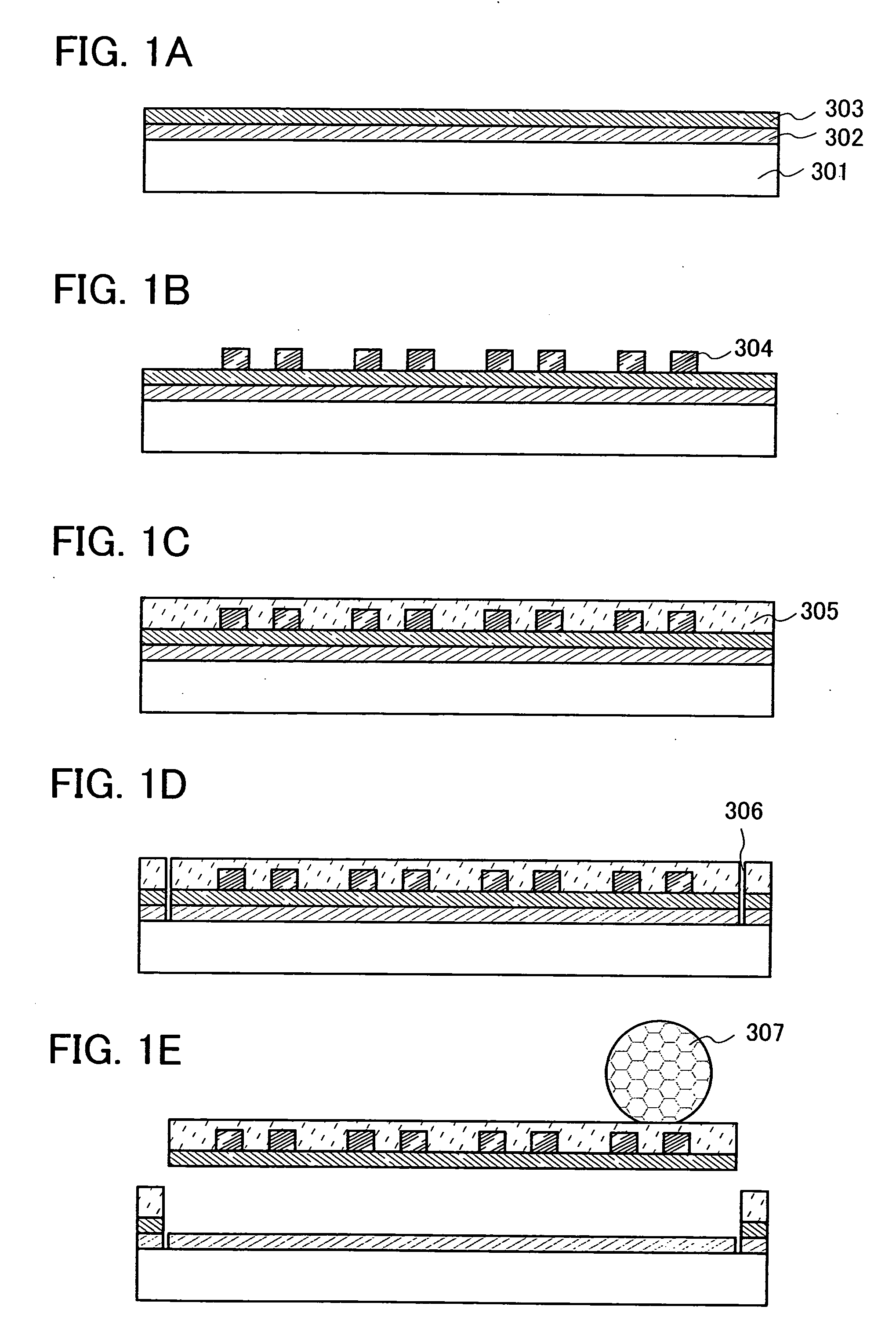
[0041]First, a separation layer 302 is formed over a substrate 301, and then, a semiconductor element layer 303 is formed (see FIG. 1A).

[0042]As the substrate 301, a glass substrate, a quartz substrate, a ceramic substrate, a metal substrate in which an insulating layer is formed on at least one surface, an organic resin substrate, or the like can be used. In this embodiment mode, a glass substrate is used as the glass substrate 301.

[0043]The separation layer 302 is formed having a single-layer structure or a stacked-layer structure of a layer with a thickness of 30 to 200 nm, which is formed using an element selected from tungsten (W), molybdenum (Mo), titanium (Ti), tantalum (Ta), niobium (Nb), nickel (Ni), cobalt (Co), zirconium (Zr), zinc (Zn), ruthenium (Ru), rhodium (Rh), palladium (Pd), osmium (Os), iridium (Ir), or silicon (Si); or ...

embodiment mode 2

[0115]In this embodiment mode, an example in which a sealing layer is formed by a manufacturing method different from that in Embodiment Mode 1 is described with reference to FIGS. 7A to 7D.

[0116]First, the manufacturing steps up to and including the step of formation of the conductive resin 304 (see FIGS. 1A and 1B) are performed based on Embodiment Mode 1. Next, the fiber body 113 is provided over the semiconductor element layer 303 (see FIG. 7A).

[0117]Then, the organic resin layer 114 is formed over the fiber body 113 and the semiconductor element layer 303. At this time, the fiber body 113 is impregnated with an organic resin in the organic resin layer 114. That is, the fiber body 113 is included in the organic resin layer 114. Accordingly, adhesion between the fiber body 113 and the organic resin layer 114 is increased.

[0118]Next, the organic resin layer 114 is heated so that the organic resin in the organic resin layer 114 is plasticized or cured. Note that when the organic re...

embodiment mode 3

[0125]In this embodiment mode, a semiconductor device having a structure different from the structures in Embodiment Modes 1 and 2 is described with reference to FIGS. 8A and 8B.

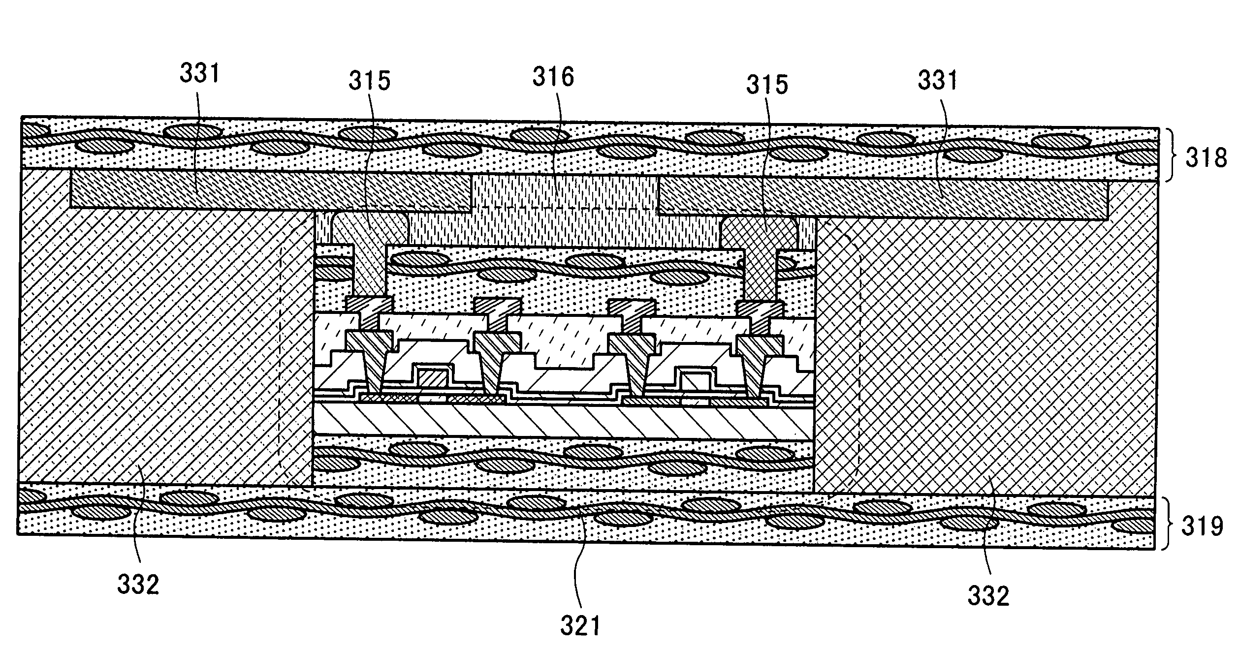
[0126]FIG. 8A is a cross-sectional view of a semiconductor device in this embodiment mode. FIG. 8B is a top plan view of FIG. 8A. An antenna 331 is provided on the substrate 318, and the chip 321 is attached to the substrate 318 with the adhesive material 316. The conductive adhesive material 315 in the chip 321 is electrically connected to the antenna 331.

[0127]The substrate 318, the antenna 331, and the chip 321 are provided with a base material 332 so as to compensate for the thickness of the chip 321. Accordingly, the thickness of the base material 332 is equal to the thickness of the chip 321, and a flat surface is formed. Moreover, the substrate 319 is attached on the flat surface.

[0128]According to this embodiment mode, a semiconductor device which has a uniform thickness and a flat surface can be obt...


PUM


Abstract

A highly reliable semiconductor device which is not damaged by local pressing force from the outside and in which unevenness of a portion where an antenna and an element overlap with each other is reduced. The semiconductor device includes a chip and an antenna. The chip includes a semiconductor element layer including a thin film transistor; a conductive resin electrically connected to the semiconductor element layer; and a sealing layer. The sealing layer in which a fiber body is impregnated with an organic resin covers the semiconductor element layer and the conductive resin, and has a thickness of 10 to 100 μm. The antenna has a depressed portion and is electrically connected to the semiconductor element layer through the conductive resin. The chip is embedded inside the depressed portion. The thickness of the chip is equal to the depth of the depressed portion.

Description

BACKGROUND OF THE INVENTION[0001]1. Field of the Invention[0002]The present invention relates to a semiconductor device and a manufacturing method thereof.[0003]2. Description of the Related Art[0004]Currently, it is important to make a variety of devices such as wireless chips and sensors into a thinner shape in miniaturizing products, and the techniques and the application range spread rapidly. Since such a variety of devices which are made thin are flexible to some extent, the devices can be mounted on an object having a curved surface.[0005]A technique of manufacturing a semiconductor device is proposed, in which an element layer including a thin film transistor, which is formed on a glass substrate, is separated from the substrate and transferred to another base material, for example, a plastic film or the like.[0006]For example, Patent Document 1 (Japanese Published Patent Application No. 2004-78991) discloses a semiconductor device in which a semiconductor chip with a size of...

Claims


Application Information

Patent Timeline
IPC IPC(8): H01L23/14
CPCH01L23/49855H01L2924/09701H01L2924/12044H01L2924/0002H01L2924/00G06K19/08G06K19/10
Inventor AOKI, TOMOYUKITSURUME, TAKUYAADACHI, HIROKIOHTANI, HISASHI
Owner SEMICON ENERGY LAB CO LTD
Why Eureka
Try Eureka