CAPACITOR HAVING Ru ELECTRODE AND TiO2 DIELECTRIC LAYER FOR SEMICONDUCTOR DEVICE AND METHOD OF FABRICATING THE SAME

a semiconductor device and capacitor technology, applied in the direction of capacitors, semiconductor devices, electrical devices, etc., can solve the problems of difficult to secure larger capacitance, limit the stability and large capacitance in narrow spaces, and difficult to deposit ternary dielectrics, etc., to achieve the effect of simple structur

Inactive Publication Date: 2009-03-12
SEOUL NAT UNIV R&DB FOUND
View PDF5 Cites 115 Cited by
  • Summary
  • Abstract
  • Description
  • Claims
  • Application Information

AI Technical Summary

Benefits of technology

[0009]The present invention provides a capacitor of a semiconductor device including a ...

Problems solved by technology

However, there is a limit to secure stable and large capacitance in narrow spaces.
Thus, the low-k layer makes it difficult to secure larger capacitance.
However, ternary dielectrics are difficult to be deposited due to their material structures, and their stoichiometries are difficult to be properly ...

Method used


Image

  • CAPACITOR HAVING Ru ELECTRODE AND TiO2 DIELECTRIC LAYER FOR SEMICONDUCTOR DEVICE AND METHOD OF FABRICATING THE SAME
  • CAPACITOR HAVING Ru ELECTRODE AND TiO2 DIELECTRIC LAYER FOR SEMICONDUCTOR DEVICE AND METHOD OF FABRICATING THE SAME
  • CAPACITOR HAVING Ru ELECTRODE AND TiO2 DIELECTRIC LAYER FOR SEMICONDUCTOR DEVICE AND METHOD OF FABRICATING THE SAME

Examples


first embodiment

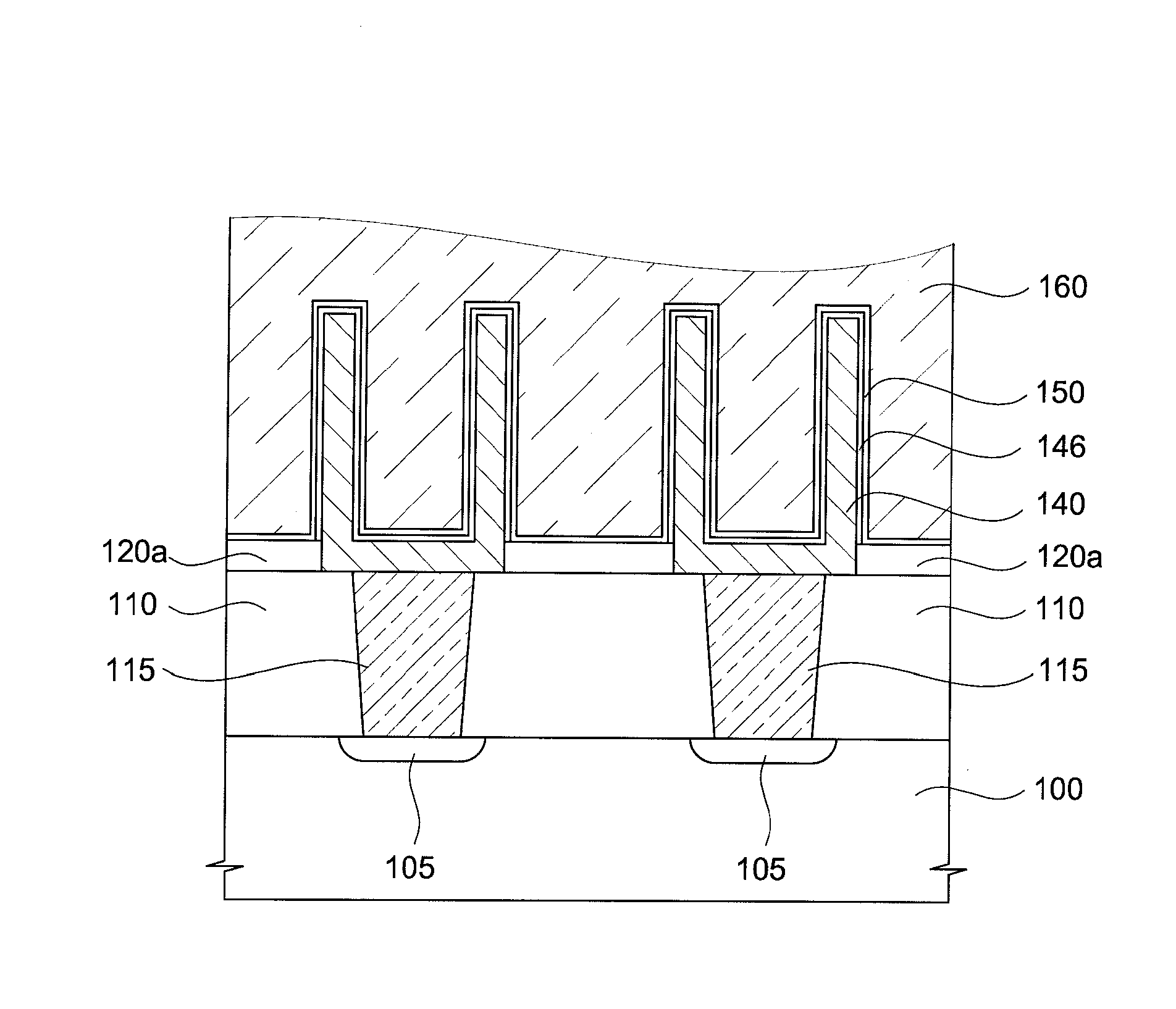
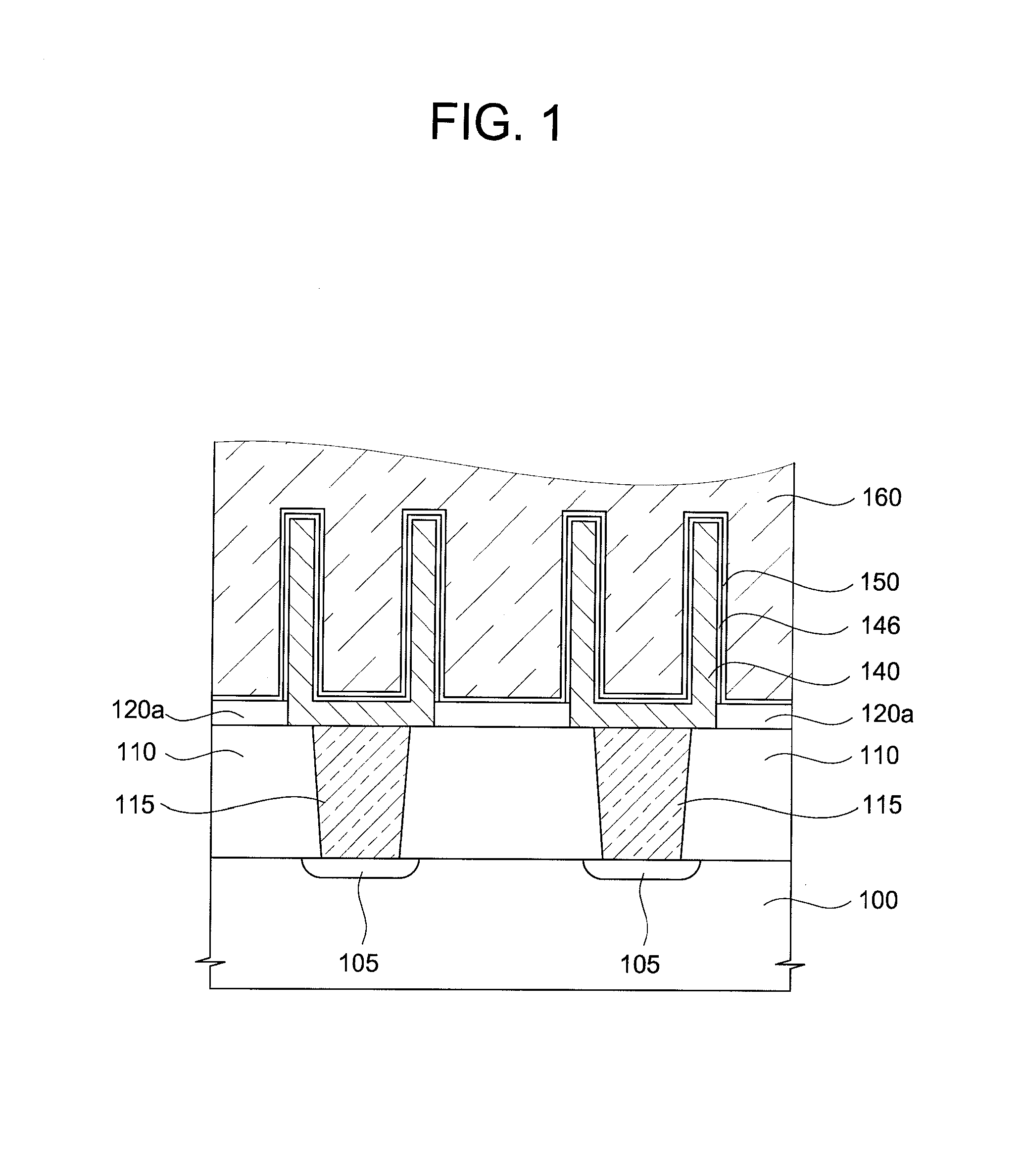
[0042]FIG. 1 is a sectional view illustrating a capacitor of a semiconductor device according to first embodiment of the present invention.

[0043]Referring to FIG. 1, a capacitor of a semiconductor device according to the present invention includes a Ru bottom electrode 140a deposited on a semiconductor substrate 100, a rutile-structured RuO2 pretreated layer 146 which is formed by oxidizing the Ru bottom electrodes 140a, a TiO2 dielectric layer 150 which is formed to have a rutile crystal structure which corresponds to the crystal structure of the RuO2 pretreated layer 146, and is doped with an impurity, and a top electrode 160 deposited on the TiO2 dielectric layer 150. The top electrode 160 can be a novel metal, a heat-resistance metal, a heat-resistance metal nitrate, or a conductive oxide. Specifically, the novel metal can be Ru, Pt, or Ir; the heat-resistance metal nitrate can be TiN, TaN, WN, TiSiN, TaSiN, TiAlN, and TaAlN; and the conductive oxide can be RuO2, IrO2, or SrRuO3...

second embodiment

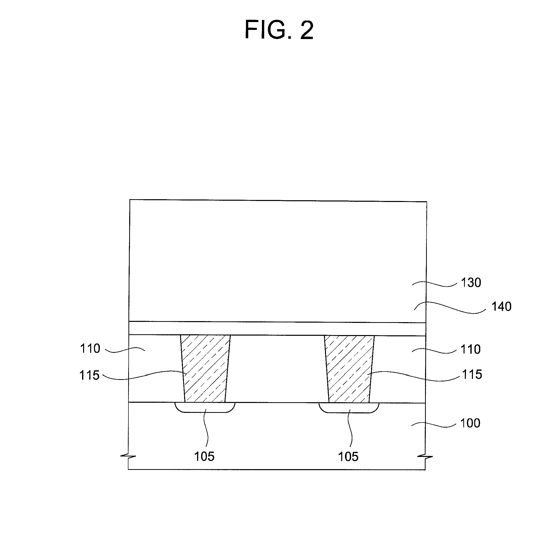
[0049]FIGS. 2 through 8 are sectional views illustrating a method of fabricating a capacitor of a semiconductor device according to second embodiment of the present invention. FIG. 9 and FIG. 10 are flow charts illustrating a process of forming a TiO2 dielectric layer in the method of fabricating a capacitor of a semiconductor device according to the second embodiment of the present invention.

[0050]Referring to FIG. 2, an active region is defined in a semiconductor substrate 100 using a device isolation process, such as a local oxidation of silicon (LOCOS) process or a shallow trench isolation (STI) process, and then a transistor structure having an impurity region 105 as source and drain is formed in the active region. The semiconductor substrate 100 used for a DRAM can be a silicon wafer in conventional cases, but is not limited thereto. For example, the semiconductor substrate 100 can be a silicon on insulator (SOI) or a silicon on sapphire (SOS).

[0051]A bottom insulating layer 1...

third embodiment

[0079]FIGS. 11 and 12 are flow charts illustrating a process of forming a TiO2dielectric layer in a method of fabricating a capacitor of a semiconductor device according to a third embodiment of the present invention.

[0080]According to the method according to the previous embodiment, the RuO2 pretreated layer 146 is formed and then, the TiO2 dielectric layer 150 is formed. However, when the TiO2 dielectric layer 150 is formed, that is, after the TiO2 dielectric layer 150 begins to be formed and before the TiO2 dielectric layer 150 is completely formed, the RuO2 pretreated layer 146 can be formed. To form the RuO2 pretreated layer 146, ozone or oxygen plasma gas can be used as an oxidant during the TiO2 dielectric layer 150 is formed. This method described above will now be described in detail.

[0081]First, the method of fabricating a capacitor is performed up to the process which has been described with reference to FIG. 5. Then, the capping layer 145 and the mold oxide layer pattern...


PUM


Abstract

Provided are a capacitor of a semiconductor device using a TiO2 dielectric layer and a method of fabricating the capacitor. The capacitor includes a Ru bottom electrode formed on a semiconductor substrate, an rutile-structures RuO2 pretreated layer which is formed by oxidizing the Ru bottom electrode, a TiO2 dielectric layer which has a rutile crystal structure corresponding to the rutile crystal structure of the RuO2 pretreated layer and is doped with an impurity, and a top electrode formed on the TiO2 dielectric layer. The method includes forming a Ru bottom electrode on a semiconductor substrate, forming a rutile-structured RuO2 pretreated layer by oxidizing a surface of the Ru bottom electrode, forming a TiO2 dielectric layer to have a rutile crystal structure corresponding to the rutile crystal structure of the RuO2 pretreated layer on the a RuO2 pretreated layer and doping the TiO2 dielectric layer with an impurity, and forming a top electrode on the TiO2 dielectric layer.

Description

BACKGROUND OF THE INVENTION[0001]1. Field of the Invention[0002]The present invention relates to a capacitor of a semiconductor device and a method of fabricating the same, and more particularly, to a capacitor of a semiconductor device having a substantially increased capacitance density and a method of fabricating the same.[0003]2. Description of the Related Art[0004]Dynamic random access memory (DRAM) which is a semiconductor device consists of one transistor and one capacitor. In order to improve capacitance of such a semiconductor device including capacitors, it is important to increase capacitance of the capacitors. Capacitance of capacitors can be increased by forming a bottom electrode as a three-dimensional structure, by increasing the height of a bottom electrode, or by reducing the thickness of a dielectric layer. However, there is a limit to secure stable and large capacitance in narrow spaces. As such, high-k dielectric layers are more demanded. Examples of a high-k mat...

Claims


Application Information

Patent Timeline
IPC IPC(8): H01L29/92H01L21/425
CPCH01L28/65H01L27/10852H10B12/033
Inventor HWANG, CHEOL SEONG
Owner SEOUL NAT UNIV R&DB FOUND
Why Eureka
Try Eureka