Method of fabrication of metal oxide semiconductor field effect transistor

a technology of field effect transistor and metal oxide, which is applied in the direction of semiconductor devices, basic electric elements, electrical equipment, etc., can solve the problems of increasing power consumption of wafers, increasing short channel effect, and increasing power consumption of each device according to the on/off frequency, so as to improve the problem of excessive spreading

Active Publication Date: 2009-03-12
UNITED MICROELECTRONICS CORP
View PDF3 Cites 54 Cited by
  • Summary
  • Abstract
  • Description
  • Claims
  • Application Information

AI Technical Summary

Benefits of technology

[0008]The present invention is directed to a method of fabrication of metal oxide semiconductor field effect transistor, for improving the issue of the excessive spreading of shallow extending dopant internally towards the channel region.
[0024]Because the method of fabrication of the metal oxide semiconductor field effect transistor of the present invention is before the forming of the source / drain extension layer, a layer of dopant diffusion barrier layer, therefore, is first formed after the forming of the source / drain extension layer, thus blocking doping due to activation of annealing to have diffusion towards the channel region. Furthermore, because the germanium composition ratio or the carbon composition ratio of the portion of the source / drain extension layer disposed adjacent to the substrate are, for example, larger than the germanium composition ratio or the carbon composition ratio disposed at the portion of the source / drain extension layer at a farther distance to the substrate, therefore, dopant, as a result of activation annealing, can thus have controlled diffusion rate of the channel region. Because the diffusion rate of the dopant towards the channel region is to achieve superior control, therefore, manufacturing allowance can be increased. Another further aspect is that because the source / drain extension layer and the source / drain layer of the metal oxide semiconductor field effect transistor of the present invention are both strained layers, therefore, the source / drain extension layer and the source / drain layer will exert stress towards the channel region, thus increasing the saturation-region drain current and the linear-region drain current of the transistor. In addition, because the material of the source / drain extension layer and the source / drain layer are silicon germanium or silicon carbide, therefore, the efficiency of the metal oxide semiconductor field effect transistor can be increased.

Problems solved by technology

Generally speaking, if other characteristics are held constant, the power consumption of each device will increase according to the on / off frequency.
Therefore, although the supply voltage and the capacitance load is decreased, the power consumption of the wafer is gradually increasing.
Furthermore, when the dimensions of the field effect transistor have become smaller, the commonly known short channel effect will become more pronounced, thus contributing to the severity of the power consumption issue.
Although the dopant diffused towards the channel region can improve, for example, punch through and other issues, the dopant diffusion rate is difficult to control, and excessive dopant will damage the transistor efficiency.
However, the ion for the halo implant will decrease the drain current, and based on the fact of continuous gate dimensional shrinkage, this issue will become more pronounced, thus disallowing the transistor efficiency to further improve.

Method used


Image

  • Method of fabrication of metal oxide semiconductor field effect transistor
  • Method of fabrication of metal oxide semiconductor field effect transistor
  • Method of fabrication of metal oxide semiconductor field effect transistor

Examples


first embodiment

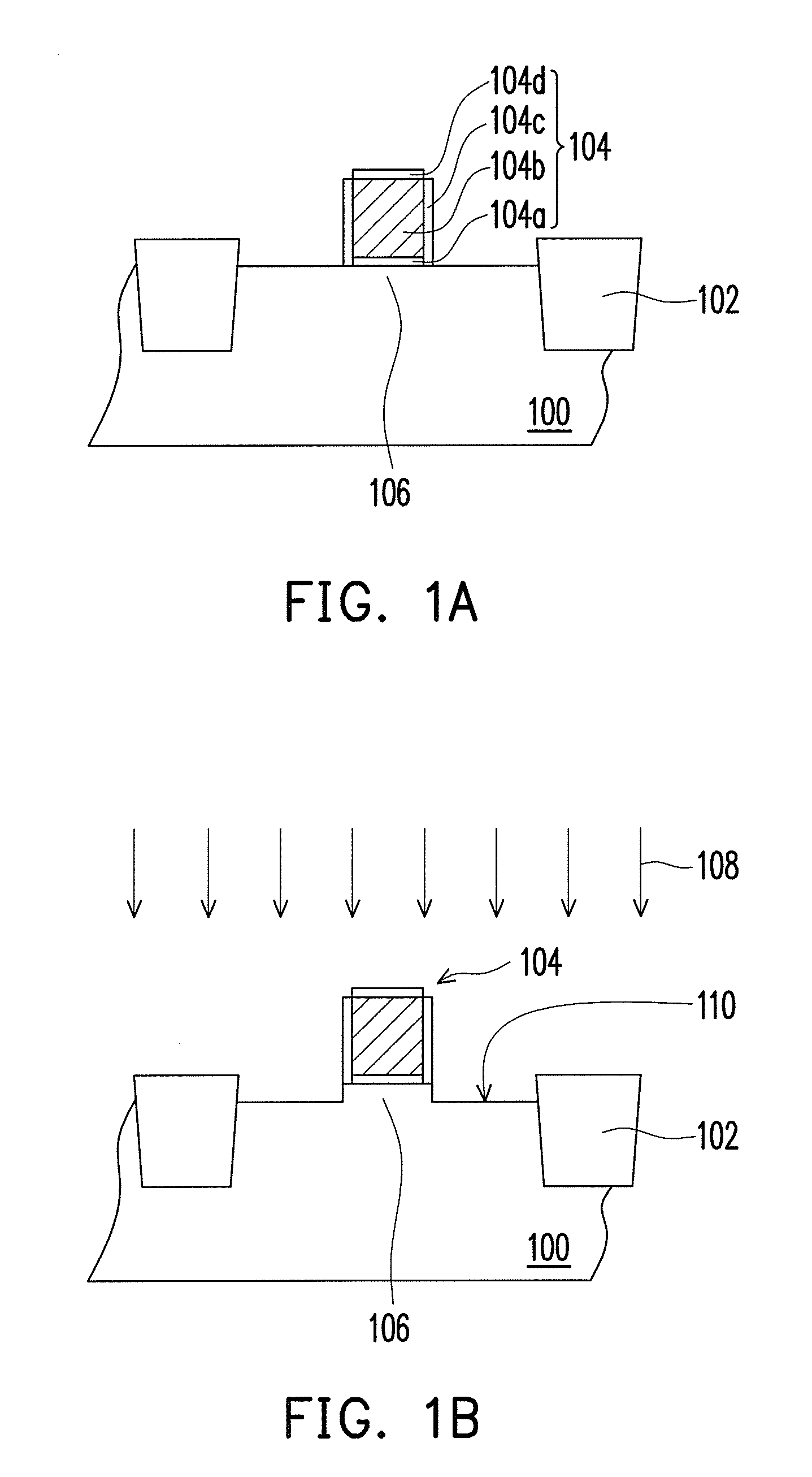
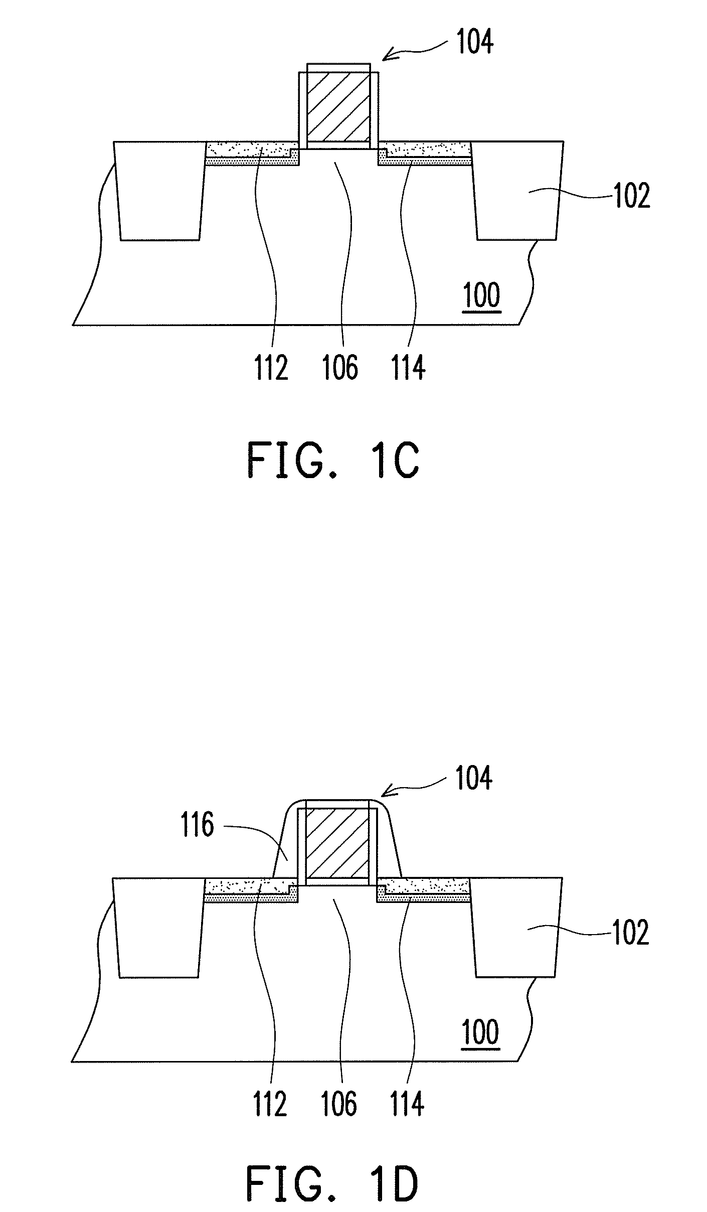
[0031]FIG. 1A to FIG. 1G are a plurality of cross-sectional views illustrating the fabrication process of the metal oxide semiconductor field effect transistor according to an embodiment of the present invention. In a first embodiment, the metal oxide semiconductor field effect transistor of the present invention is using a PMOS process as an illustrative example.

[0032]Referring to FIG. 1A, a substrate 100 is first provided, where the substrate 100, for example, is silicon-based substrate, pure silicon substrate, silicon on insulator (SOI) substrate, germanium channel substrate, substrate having bulk strain, and substrate having crystallographic orientation. A plurality of isolation structures 102 are formed on the substrate 100. The material of the isolation structure 102, for example, is silicon oxide. A gate structure 104 is formed on the substrate 100 in between the isolation structures 102. The gate structure 104 at least includes the gate dielectric layer 104a, the gate 104b, ...

second embodiment

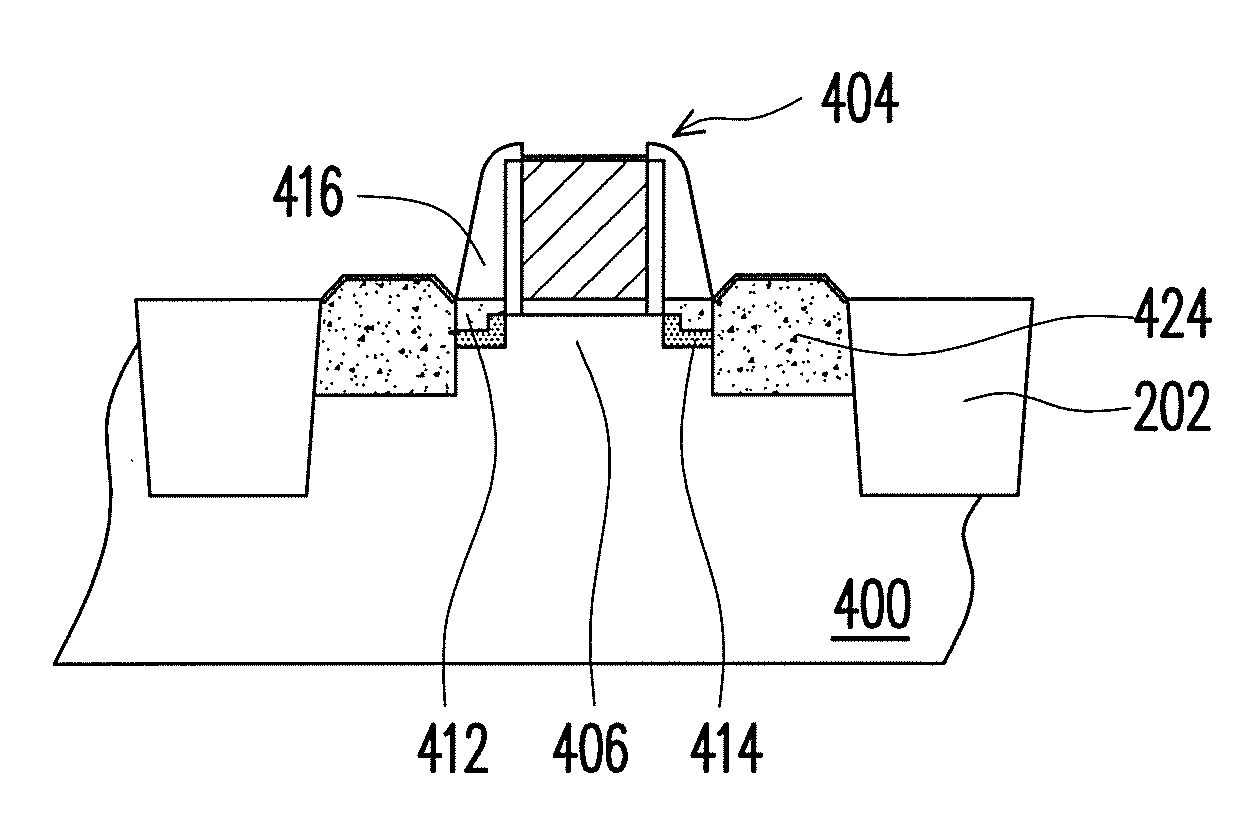
[0042]FIG. 2 is a cross-sectional view of the metal oxide semiconductor field effect transistor, according to another embodiment of the present invention.

[0043]Referring to FIG. 2, this metal oxide semiconductor field effect transistor primarily includes a substrate 200, an isolation structure 202, a gate structure 204, a spacer 216, a source / drain extension layer 212, and a source / drain layer 224. The substrate 200, for example, is silicon-based substrate, silicon on insulator (SOI) substrate, germanium channel substrate, substrate having bulk strain, and substrate having crystallographic orientation. The gate structure 204 is disposed on the substrate 200 in between the isolation structures 202. The portion of the substrate 200 below the gate structure 204 is the channel region of the metal oxide semiconductor field effect transistor. The spacer 216 is disposed on the side wall of the gate structure 204. The source / drain extension layer 212 is disposed in the substrate 200 under t...

third embodiment

[0047]FIG. 3A to FIG. 3G are a plurality of cross-sectional views illustrating the fabrication process of the metal oxide semiconductor field effect transistor according to another embodiment of the present invention.

[0048]In the third embodiment, a NMOS fabrication process is described as an example for the illustration of the metal oxide semiconductor field effect transistor of the present invention.

[0049]Referring to FIG. 3A, first a substrate 300 is provided. The substrate 300, for example, is silicon-based substrate, silicon on insulator (SOI) substrate, germanium channel substrate, substrate having bulk strain, and substrate having crystallographic orientation. A plurality of isolation structures 302 are formed on the substrate 300. The material of the isolation structure 302, for example, is silicon oxide. A gate structure 304 is formed on the substrate 300 in between the isolation structures 302. The gate structure 304 at least includes a gate dielectric layer 304a, a gate 3...


PUM


Abstract

A method of fabrication of a metal oxide semiconductor field effect transistor includes first providing a substrate on which a gate structure is formed. Afterwards, a portion of the substrate is removed to form a first recess in the substrate at both ends of the gate structure. Additionally, a source / drain extension layer is deposited in the first recess and a number of spacers are formed at both ends of the gate structure. Subsequently, a portion of the source / drain extension and the substrate are removed to form a second recess in the source / drain extension and a portion of the substrate outside of the spacer. In addition, a source / drain layer is deposited in the second recess. Because the source / drain extension and the source / drain layer have specific materials and structures, short channel effect is improved and the efficiency of the metal oxide semiconductor field effect transistor is improved.

Description

CROSS-REFERENCE TO RELATED APPLICATION[0001]This application is a divisional of an application Ser. No. 11 / 308,718, filed on Apr. 26, 2006, now pending. The entirety of the above-mentioned patent applications is hereby incorporated by reference herein and made a part of this specification.BACKGROUND OF THE INVENTION[0002]1. Field of Invention[0003]The present invention is related to a semiconductor device and its method of fabrication, especially is related to a method of fabrication of a metal oxide semiconductor field effect transistor having strained layer.[0004]2. Description of Related Art[0005]The semiconductor industry and wafer fabrication is headed towards higher efficiency and ultra large-scale integration. For the sake of accomplishing higher effectiveness using the same amount of footprint area, the wafer characteristic dimensions and supply voltage will continue to diminish. Generally speaking, if other characteristics are held constant, the power consumption of each de...

Claims


Application Information

Patent Timeline
Patent Type & Authority Applications(United States)
IPC IPC(8): H01L21/336
CPCH01L21/823807H01L29/6656H01L29/7848H01L29/7834H01L29/66636Y10S438/931Y10S438/933Y10S438/938
Inventor TSAI, CHEN-HUALAN, BANG-CHIANGLIN, YU-HSINLIU, YI-CHENGTSAI, CHENG-TZUNG
Owner UNITED MICROELECTRONICS CORP
Why Eureka
Try Eureka