Field effect transistor

a field effect transistor and transistor technology, applied in the direction of solid-state devices, thermoelectric devices, material analysis, etc., can solve the problems of significant shift in threshold voltage and general poor driving stability of devices employing organic semiconductors, and achieve high current driving capability, increase driving stability, and increase mobility

Inactive Publication Date: 2009-03-19
MITSUBISHI CHEM CORP
View PDF10 Cites 19 Cited by
  • Summary
  • Abstract
  • Description
  • Claims
  • Application Information

AI Technical Summary

Benefits of technology

[0015]According to the present invention, a field effect transistor which has an organic semiconductor portion formed by employing an organic semiconductor solution, the organic semiconductor portion having increased driving stability and which thereby has long lifer and a display device and an electronic circuit employing it, can be provided.
[0016]Further, according to the present invention, a field effect transistor which has an organic semiconductor portion formed by employing an organic semiconductor solution, the organic semiconductor portion having an increased mobility, and which thereby has high current driving capability, can be provided.

Problems solved by technology

However, a device employing an organic semiconductor has been known to be generally poor in driving stability as compared with an inorganic semiconductor device.
However, in a case of a field effect transistor employing an organic material such as pentacene or a polyfluorene polymer for the semiconductor, the shift in the threshold voltage is significant, such being practically problematic (Non-Patent Documents 1 to 3).

Method used


Image

  • Field effect transistor
  • Field effect transistor
  • Field effect transistor

Examples


preparation example 1

Preparation of Bicycloporphyrin Copper Complex

[0131]In accordance with a method as disclosed in S. Ito; N. Ochi, T. Murashima, H. Uno, N. Ono, Heterocycles, vol. 52, 399 (2000), a copper bicycloporphyrin complex was prepared from bicycloporphyrin in the following route Namely, 92.8 mg (0.16 mmol) of bicycloporphyrin having the following structure and 313.6 mg (1.6 mmol) of coppery(II) acetate dihydrate were dissolved in a mixed liquid of chloroform 151 mL / methanol 15 mL, followed by stirring for about one hour. It was confirmed by alumina TLC (eluting solvent: chloroform / hexane=1 / 1) that the materials disappeared and a novel compound formed. Accordingly, water was added to terminate the reaction, washing with water was carried out as it was, and an organic layer was separated. Further, the organic layer was washed with a saturated salt solution and dried over anhydrous sodium sulfate. The drying agent was removed by filtration with a filter paper, and then the solvent was distilled ...

preparation example 2

Preparation of Bicycloporphyrin

[0133]Bicycloporphyrin was prepared in accordance with a method as disclosed in S. Ito, N. Ochi, T. Murashima, H. Uno, N. Ono, Heterocycles, vol. 52, 399 (2000) in the following route.

Diels-Alder Reaction

[0134]

[0135]Into a 2 L four-necked flask equipped with a reflux condenser, trans-1,2-diphenylsulfonylethylene (52.74 g, 171 mmol) was put and dispersed in 1.6 L of toluene. Then, 1,3-cyclohexadiene (20.52 mL 205.2 mmol) was put in this solution, followed by reflux for 5 hours to carry out a heat diels-alder reaction. After completion of the reaction, vacuum concentration was carried out by an evaporator, followed by washing with hexane to obtain 72 g (yield: 99%) of 2-exo,3-endo-bis(phenylsulfonyl)bicyclo[2.2.2]oct-5-ene as an aimed product. As the measure of completion of the reaction the completion of the reaction was judged by complete dissolution of trans-1,2-diphenylsulfonylethylene as the material dispersed in toluene, and disappearance of the pe...

preparation example 3

Preparation of Bicycloporphyrin Copper Complex

[0142]The same operation as in Preparation Example 1 was carried out except that chromatography by an alumina gel was not carried out in preparation of the bicycloporphyrin copper complex, to obtain a bicycloporphyrin copper complex

Measurement of Purity of Organic Semiconductor Materials

[0143]Purities of the porphyrin materials obtained in Preparation Examples 1 to 3 and pentacene (manufactured by TOKYO KASEI KOGYO Co., Ltd) were measured by means of CHN elemental analysis method. With respect to pentacene, one formed by sublimation was employed.

[0144]Purities of the organic semiconductors were measured by means of a combustion-thermal conductivity method employing as a CHN measuring apparatus PERKIN ELMER 2400 Series II CHN / O Analyzer. As a method of calculating the purity, each semiconductor was held in a vacuum of 10−5 Torr for 3 hours to remove the solvent and moisture so as to eliminate disturbance factors, and then subjected to CHN...


PUM


Abstract

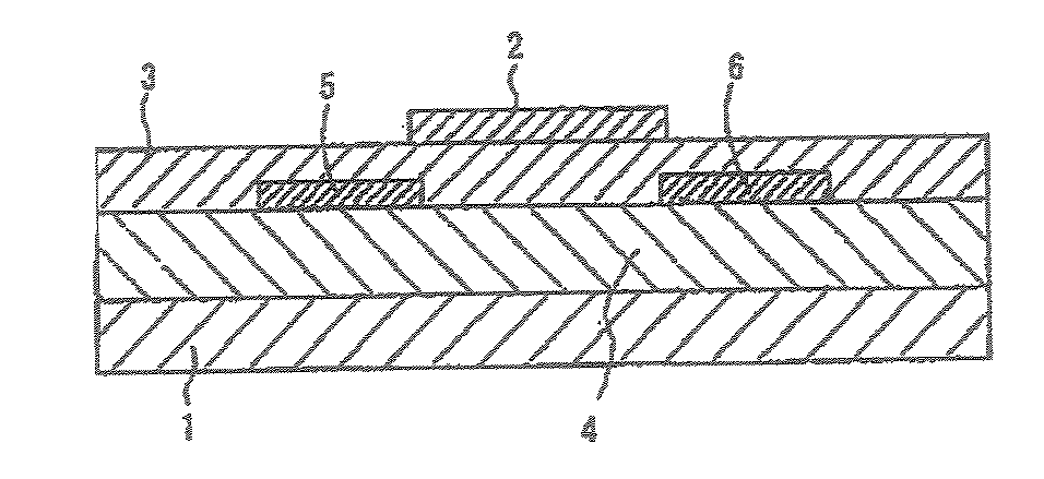
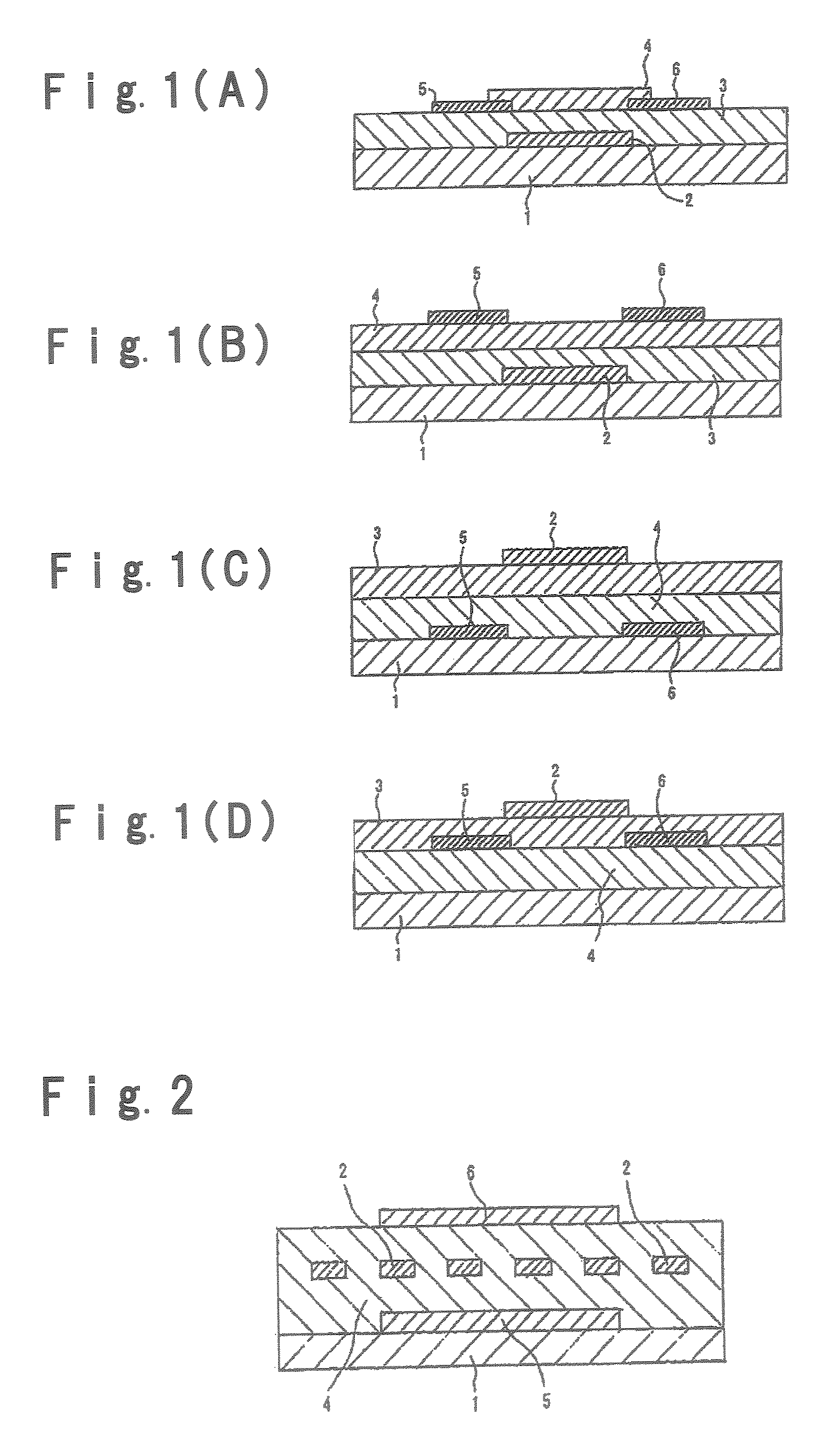
A field effect transistor including a gate isulation portion, an organic semiconductor portion, a source electrode and a drain electrode, wherein when a voltage is applied to the gate at 70° C. for 5.0±0.1 hours so that the field strength in the gate insulation portion would be 100±5 MV/m, the change in the threshold voltage is within 5 V. The organic semiconductor portion has a high driving stability, of which the change in characteristics by driving is thereby small.

Description

TECHNICAL FIELD[0001]The present invention relates to a field effect transistor. More particularly, it relates to a field effect transistor having an organic semiconductor portion formed by employing an organic semiconductor.BACKGROUND ART[0002]In a field effect transistor comprising a support substrate, and a gate electrode and a semiconductor portion separated by a gate insulation portion, a source electrode and a drain electrode provided so as to contact the semiconductor portion formed on the support substrate, an organic material is used for the semiconductor portion. The organic material attracts attention because the semiconductor portion can be formed by application of its solution, and weight reduction can be achieved and impact strength can be imparted by use of e.g. a polymer, in addition to advantage in view of cost over a conventional formation process by e.g. vacuum process employing an inorganic material such as a silicon.[0003]However, a device employing an organic s...

Claims


Application Information

Patent Timeline
Patent Type & Authority Applications(United States)
IPC IPC(8): H01L51/10H01L51/40
CPCH01L21/3127H01L51/0077H01L51/0512H01L51/052Y10T436/107497H01L51/0545H01L51/0558Y10T436/148888H01L51/0541H01L21/02282H01L21/0212H10K85/30H10K10/462H10K10/471H10K10/466H10K10/464H10K10/484
Inventor ARAMAKI, SHINJIYOSHIYAMA, RYUICHIOHNO, AKIRASAKAI, YOSHIMASA
Owner MITSUBISHI CHEM CORP
Why Eureka
Try Eureka