Field-effect transistor, semiconductor chip and semiconductor device

a field-effect transistor and semiconductor chip technology, applied in semiconductor devices, semiconductor/solid-state device details, electrical apparatus, etc., can solve the problems of poor productivity, difficult to meet this requirement, and poor homogeneity of the wafer surface and reproducibility between wafers, etc., to achieve uniform fet characteristics, high precision, and good productivity

Inactive Publication Date: 2009-03-26
RENESAS ELECTRONICS CORP
View PDF9 Cites 74 Cited by
  • Summary
  • Abstract
  • Description
  • Claims
  • Application Information

AI Technical Summary

Benefits of technology

[0049]In accordance with the present invention, the structure of a single-step recess is realized using a wet-etching stop layer, as a result of which good productivity and a uniform FET characteristic are obtained. Further, the channel layer of the FET is managed with a high precision by the epitaxial growth technique of the semiconductor layer. This precision improves the electrical characteristics of the FET. By using the etching stop layer, it is unnecessary to adjust depth by repeatedly cutting a recess while measuring current value using monitor elements. This makes it possible to improve productivity and the accuracy of the FET characteristics.
[0050]Further, recess formation without using an etching stop layer is isotropic and side etching in the lateral direction cannot be controlled independently. However, in the FET of the present invention, side etching in the lateral direction can be controlled independently by using an etching stop layer. That is, since the spacing between the gate electrode and contact layer can be controlled, adjustment can be performed so as to obtain high-frequency performance. Further, lateral side etching utilizing the etching stop layer is a trace amount of etching within a slender (thin) gap. Therefore, in comparison with recess forma

Problems solved by technology

Consequently, it is required that etching and current measurement be repeated, resulting in poor productivity.
Further, owing to such etching, homogeneity in the wafer surface and reproducibility between wafers are not so

Method used


Image

  • Field-effect transistor, semiconductor chip and semiconductor device
  • Field-effect transistor, semiconductor chip and semiconductor device
  • Field-effect transistor, semiconductor chip and semiconductor device

Examples


first exemplary embodiment

; Method of Manufacturing FET)

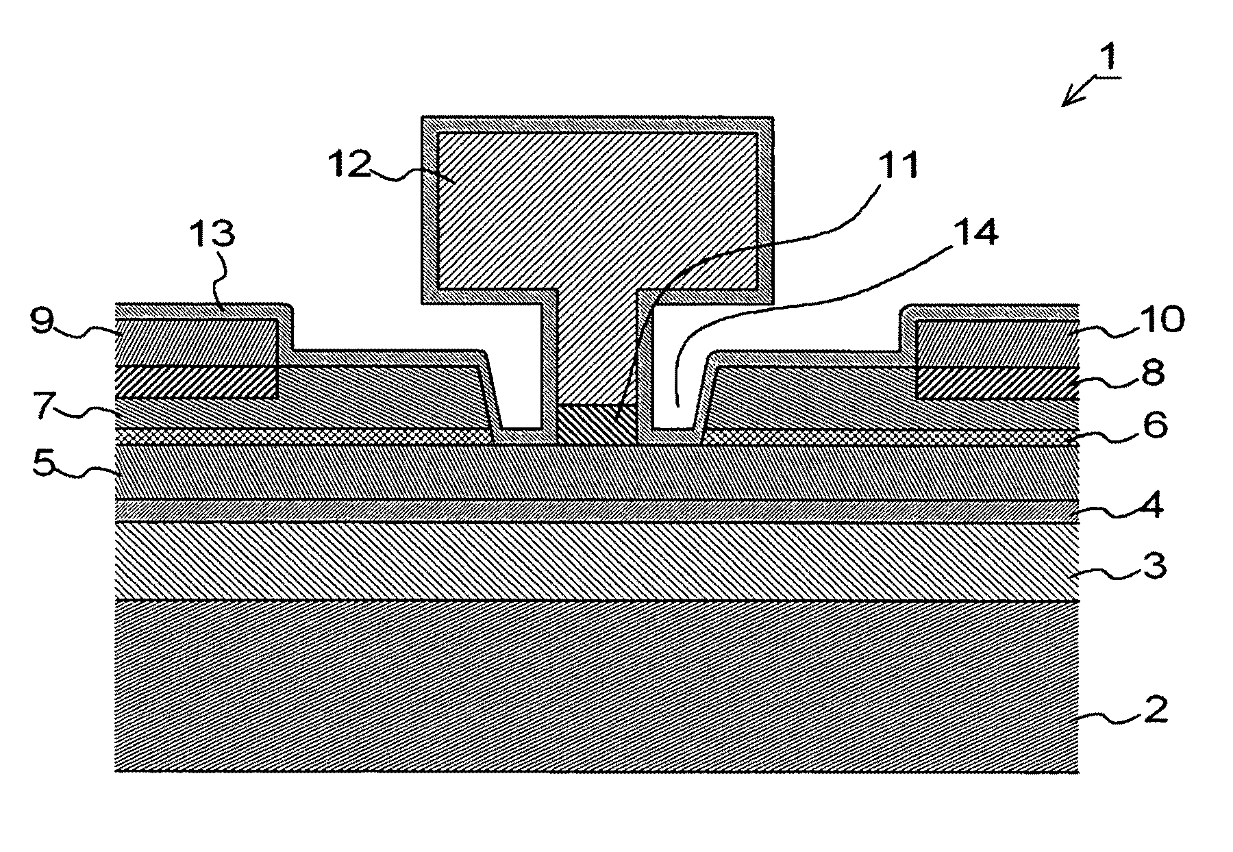
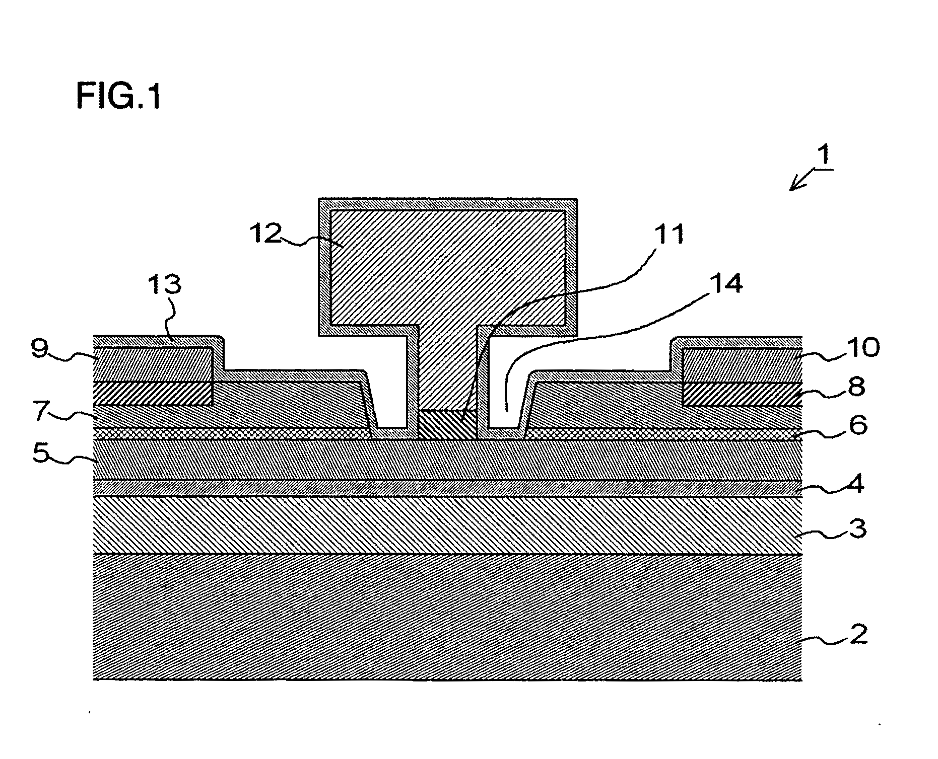
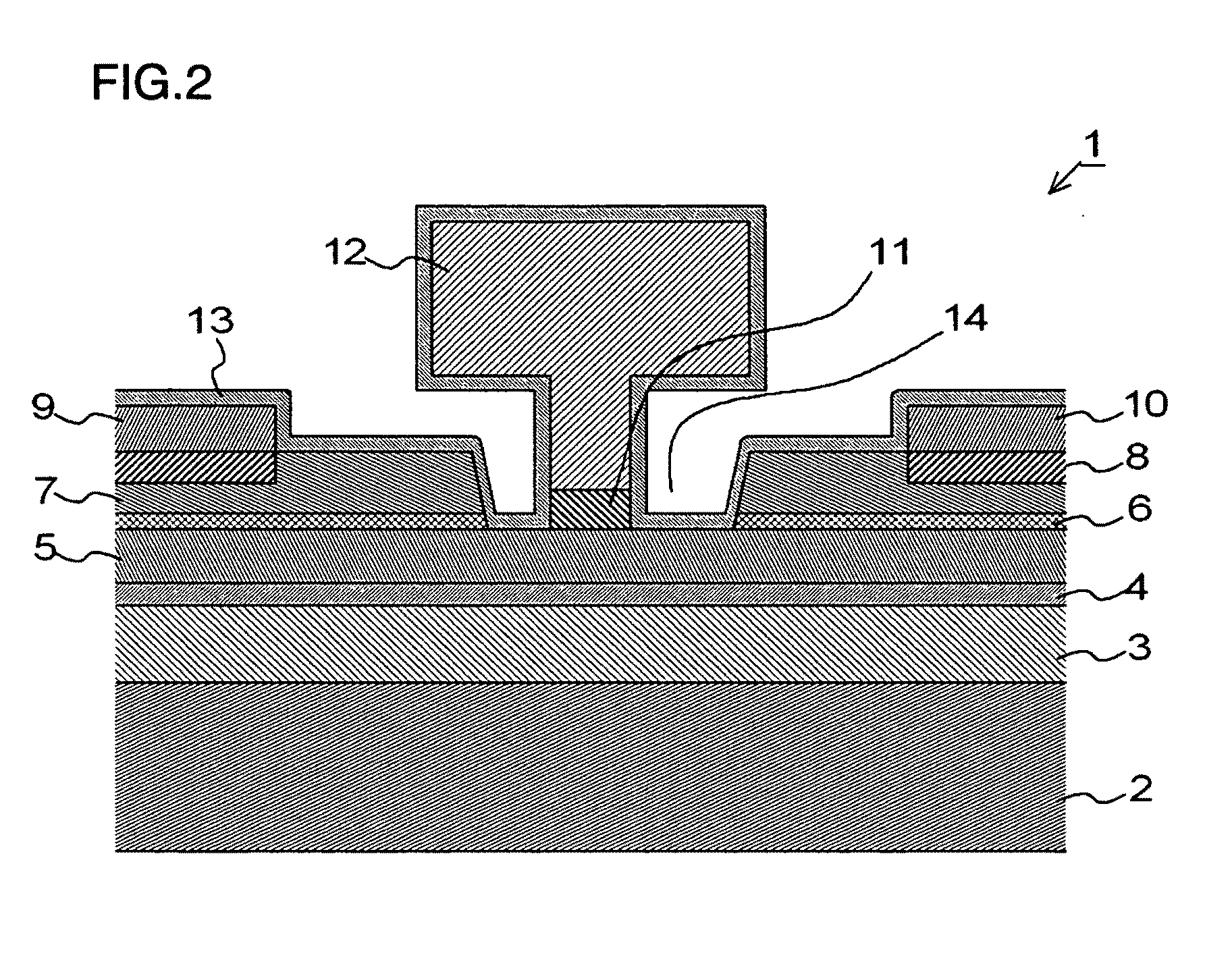
[0127]Next, a method of manufacturing a FET according to an exemplary embodiment of the present invention will be described. FIGS. 10A to 10H are sectional views useful in describing basic steps up to formation of FET electrodes as a method of manufacturing the FET (FIG. 1) according to the first exemplary embodiment. Although the FET shown in FIGS. 10A to 10H has portions that differ in terms of particulars from those of the FET shown in the sectional view of FIG. 1, there is no intent to show an absence of correlation with regard to the FET shown in FIG. 1 and the FET illustrated in FIGS. 10A to 10H. Further, the numerical values of the conditions represent one example and the invention is not limited to these values.

[0128]First, the i-type GaAs layer 3 (thickness: 500 nm) serving as the buffer layer, the i-type InGaAs layer 4 (thickness: 13 nm) serving as the two-dimensional electron gas layer, the n-type AlGaAs layer 5 (thickness: 33 nm) serving as ...

seventh exemplary embodiment

; Flip-Chip Mounting of Semiconductor Chip

[0191]A semiconductor device in which the semiconductor chip of the present invention is flip-chip-mounted directly on a circuit board will be described next as a seventh exemplary embodiment of the present invention. FIG. 19 is a top plan view of a semiconductor device 101, and FIG. 20 is a sectional view taken along line B-B of FIG. 19.

[0192]A multistage amplifier extending from low-noise amplification of input to an output section, a plurality of multistage amplifiers inclusive of switch changeover and various circuits that include multiple functions such as modulation and digital processing can be used as the circuits of the semiconductor device 101. A semiconductor chip 102 may be an MMIC or the like obtained by packaging FETs or passive elements (capacitors and inductors, etc.).

[0193]In the semiconductor device 101, wiring such as of gold (Au) or copper (Cu) is formed on the surface of a circuit board 103 made of a resin or ceramic suc...


PUM


Abstract

A FET exhibiting excellent uniformity and productivity and having a low noise figure and high associated gain as high-frequency performance, a semiconductor chip having this FET and a semiconductor device having the semiconductor chip. The FET includes a GaAs substrate on which are built up an i-type GaAs layer, an i-type InGaAs two-dimensional electron gas layer and an n-type AlGaAs electron supply layer. A gate electrode is provided on and in linear Schottky contact with the n-type AlGaAs electron supply layer. A n-type InGaP etching stop layer and then an n-type GaAs contact layer at the same lateral position are built up on the n-type AlGaAs electron supply layer, these being spaced away from both sides of the gate electrode. A source electrode and a drain electrode are provided on the n-type GaAs contact layer and are spaced away from edges of the contact layer as electrodes that make band-shaped ohmic contact.

Description

REFERENCE TO RELATED APPLICATION[0001]This application is based upon and claims the benefit of the priority of Japanese patent application No. 2007-247574, filed on Sep. 25, 2007, the disclosure of which is incorporated herein in its entirety by reference thereto.TECHNICAL FIELD[0002]This invention relates to a field-effect transistor of Schottky-coupled-gate type and, more particularly, to a field-effect transistor formed on a gallium-arsenide substrate. Further, the invention relates to a semiconductor chip having such a field-effect transistor and to a semiconductor device having this semiconductor chip.BACKGROUND[0003]The spread of satellite broadcasts and microwave communications has been accompanied by increasing demand for low-noise amplification elements used in the first stage of the high-frequency amplifying circuit that receives the signal. In particular, field-effect transistors (FETs) formed on a gallium-arsenide (GaAs) substrate are primarily used for satellite broadca...

Claims


Application Information

Patent Timeline
IPC IPC(8): H01L29/778H01L23/48
CPCH01L29/66462H01L29/7783H01L2224/48091H01L2224/48247H01L2224/48257H01L2924/13062H01L2924/00014H01L2924/00H01L2924/12032H01L29/41758H01L29/772H01L29/812
Inventor ASAI, SHUJIFUJIHARA, AKIRAMATSUNOSHITA, MAKOTOSAKURA, NAOKIICHIKAWA, SEIJI
Owner RENESAS ELECTRONICS CORP
Why Eureka
Try Eureka