Semiconductor device
- Summary
- Abstract
- Description
- Claims
- Application Information
AI Technical Summary
Benefits of technology
Problems solved by technology
Method used
Image

Examples
first embodiment
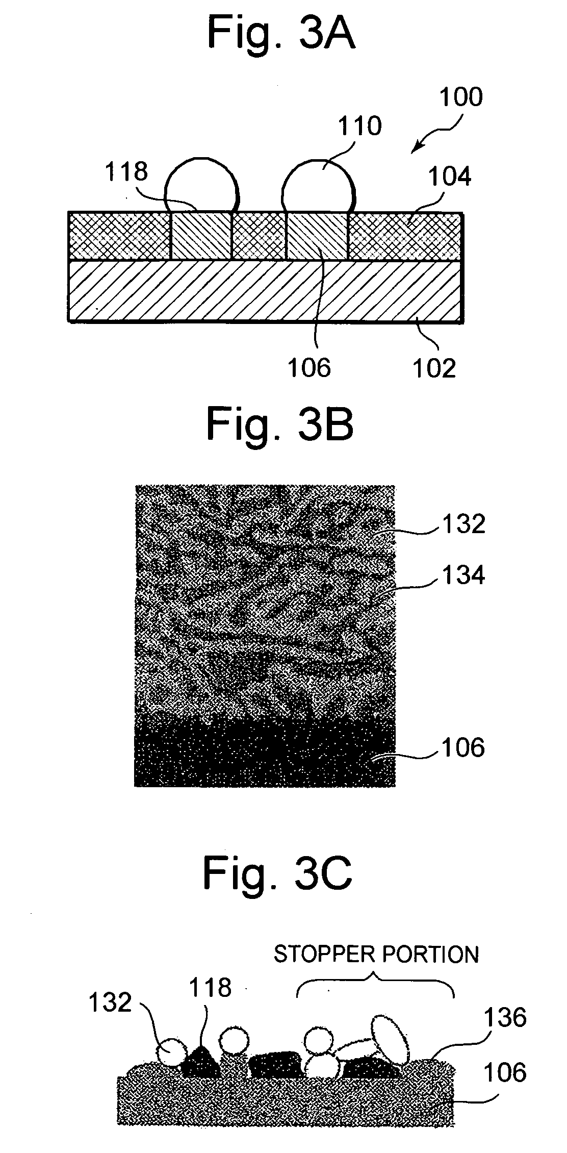
[0075]In a first embodiment, a semiconductor device was manufactured in which the alloy composition of each external connecting terminal of the semiconductor device was SnBi (Sn: 59 wt % and Bi: 41 wt %) and each stopper portion was provided around a Cu electrode and each intermetallic compound.
(Fabrication of Semiconductor Device)
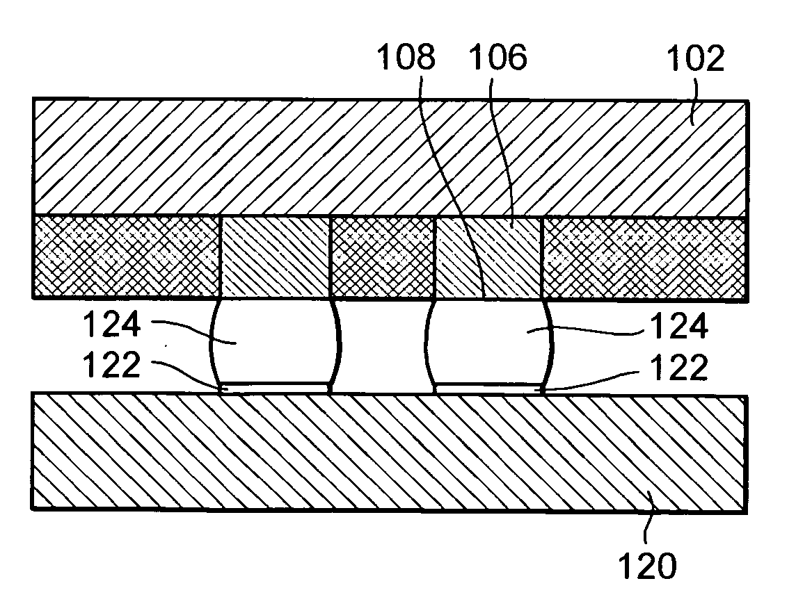
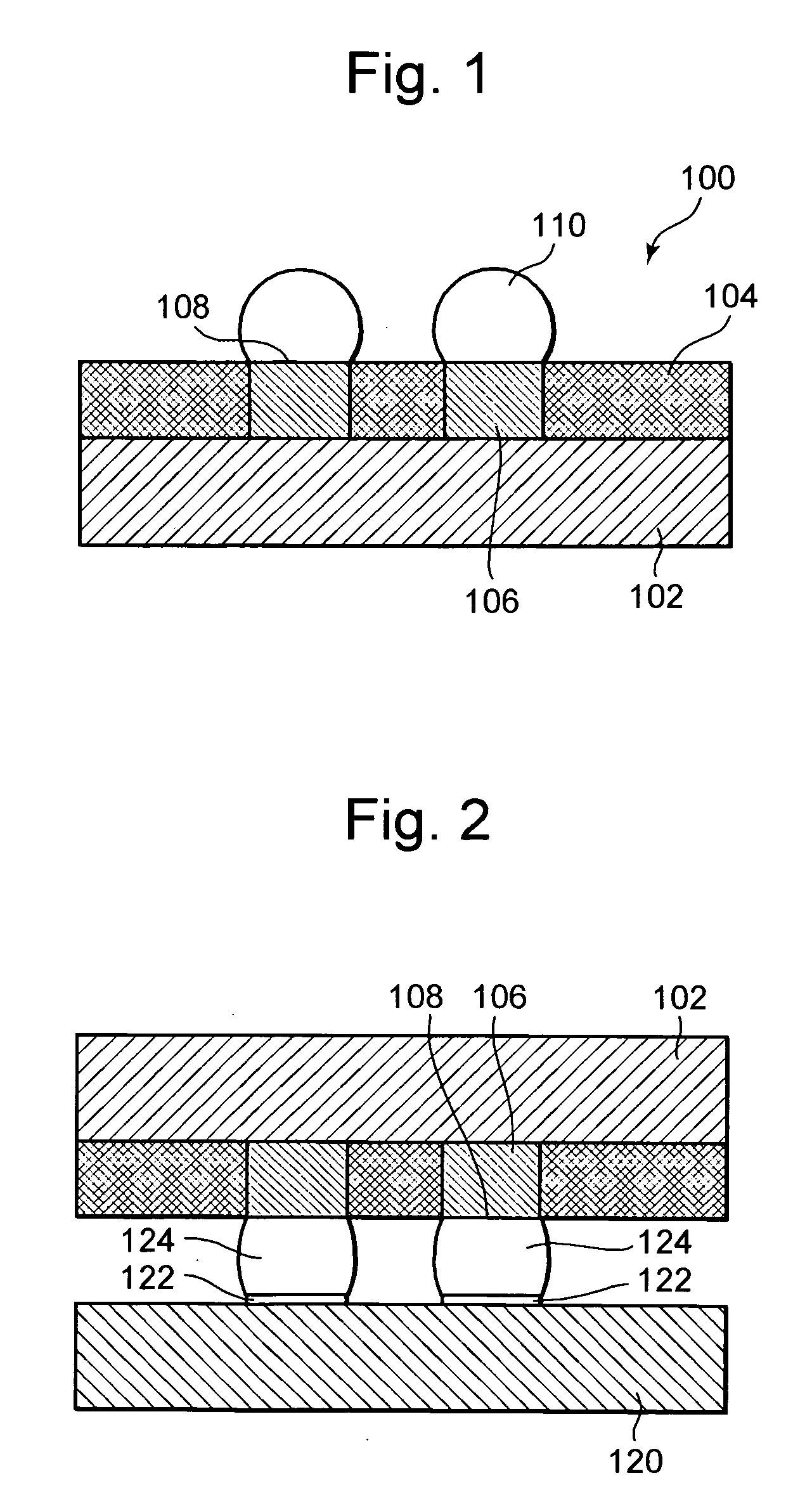
[0076]The present embodiment will be described along FIG. 5. The known wafer process is performed on the corresponding substrate 102 to form a semiconductor chip in which wirings are arranged in matrix form. Thereafter, an insulating resin composed of polyimide is applied onto the semiconductor chip by spin coating and then dried, thereby forming an insulating layer (not shown) of 5 μm. Then, an area other than electrode pads is covered with a mask to expose the electrode pads. After exposure, development processing was conducted to expose the electrode pads. Next, a seed layer composed of titanium or the like is formed by an ion sputter method. Then, copp...
fifth embodiment
[0085]A semiconductor device obtained by performing processing as in the first embodiment is mounted on its corresponding mounting board. Its mounting method will be described below.
(Mounting of Semiconductor Device on Mounting Board)
[0086]Solder paste having a composition of Sn(100-x-y)AgxCuy (where x=3 wt % and y=0.5 wt %) is printed on each electrode pad (material: copper) formed in a mounting board (QSX-33398: made by Eastern Co., Ltd.) composed of a compound of glass and an epoxy resin via a metal mask interposed therebetween. Thereafter, each connecting terminal of the semiconductor device is mounted on the solder paste and a reflow process (XNIII-725PC(b): made by Furukawa Electric Co., Ltd.) is performed to mount the semiconductor device on the mounting board.
[0087]Incidentally, the condition for the reflow process was that the temperature rise / drop rate was 2.5° C. / minute, the peak temperature was 240° C. and the holding time at 220° C. was one minute. The composition of t...
eighth embodiment
[0090]After the semiconductor device has been mounted on the mounting board in the fifth embodiment, a temperature cycle process shown below is conducted, and the thickness of each intermetallic compound and the proportion of each stopper portion were evaluated in a manner similar to the fifth embodiment. Thermal shock reliability, a repetitive bending fracture cycle ratio and a repetitive drop fracture cycle ratio such as shown below were evaluated. The result thereof is shown in Table 3.
Thermal Shock Reliability
[0091]One in which the semiconductor device has been mounted onto the mounting board is inserted into a thermal shock test chamber (TSA-101S-W: made by ESPEC Co., Ltd.) and left in the atmosphere under a temperature cycle condition shown in FIG. 6. The electric resistance value of a junction between the semiconductor device and the mounting board is measured in real time simultaneously with the start of a temperature cycle. Next, electric resistance values on the high-temp...
PUM
 Abstract
Description
Claims
Application Information