Means for improved implementation of laser diodes and laser diode arrays

a laser diode array and laser diode technology, applied in lasers, semiconductor lasers, solid-state devices, etc., can solve the problems of large “built-in” residual stresses that can have detrimental effects on the performance of semiconductor laser diode devices, reduce reliability, and significant built-in stresses between mated substrates, so as to achieve better cooling or higher performance

Active Publication Date: 2009-04-09
HUFF MICHAEL +1
View PDF5 Cites 49 Cited by
  • Summary
  • Abstract
  • Description
  • Claims
  • Application Information

AI Technical Summary

Benefits of technology

[0019]The present invention is also directed to improved methods of merging a semiconductor substrate containing laser diode or laser d

Problems solved by technology

The use of intermediate layer(s) made from the solders and adhesives that are commonly used for joining laser diode semiconductor substrates to metal substrates can result in large “built-in” residual stresses that can have detrimental effects on the performance of the semiconductor laser diode devices.
The differing thermal expansion coefficients of the metal and semiconductor substrates, combined with the elevated temperatures required to perform the soldering process, as well as thermal stresses resulting from the heating of the laser diodes when operating, can result in significant built-in stresses between the mated substrates once they are cooled to room temperature, as well as during operation.
Large built-in stresses have also been known to appreciably lower the reliability of semiconductor laser diode devices, which frequently heat-up due to the power dissipated during operation, thereby resulting in large thermal stresses developing between the mated semiconductor and metal substrates.
The thermal stress can become sufficiently large so as to result in the fracture of the semiconductor substrate and/or the substrates breaking or coming apart due to a failure at the soldered

Method used


Image

  • Means for improved implementation of laser diodes and laser diode arrays
  • Means for improved implementation of laser diodes and laser diode arrays
  • Means for improved implementation of laser diodes and laser diode arrays

Examples


Embodiment Construction

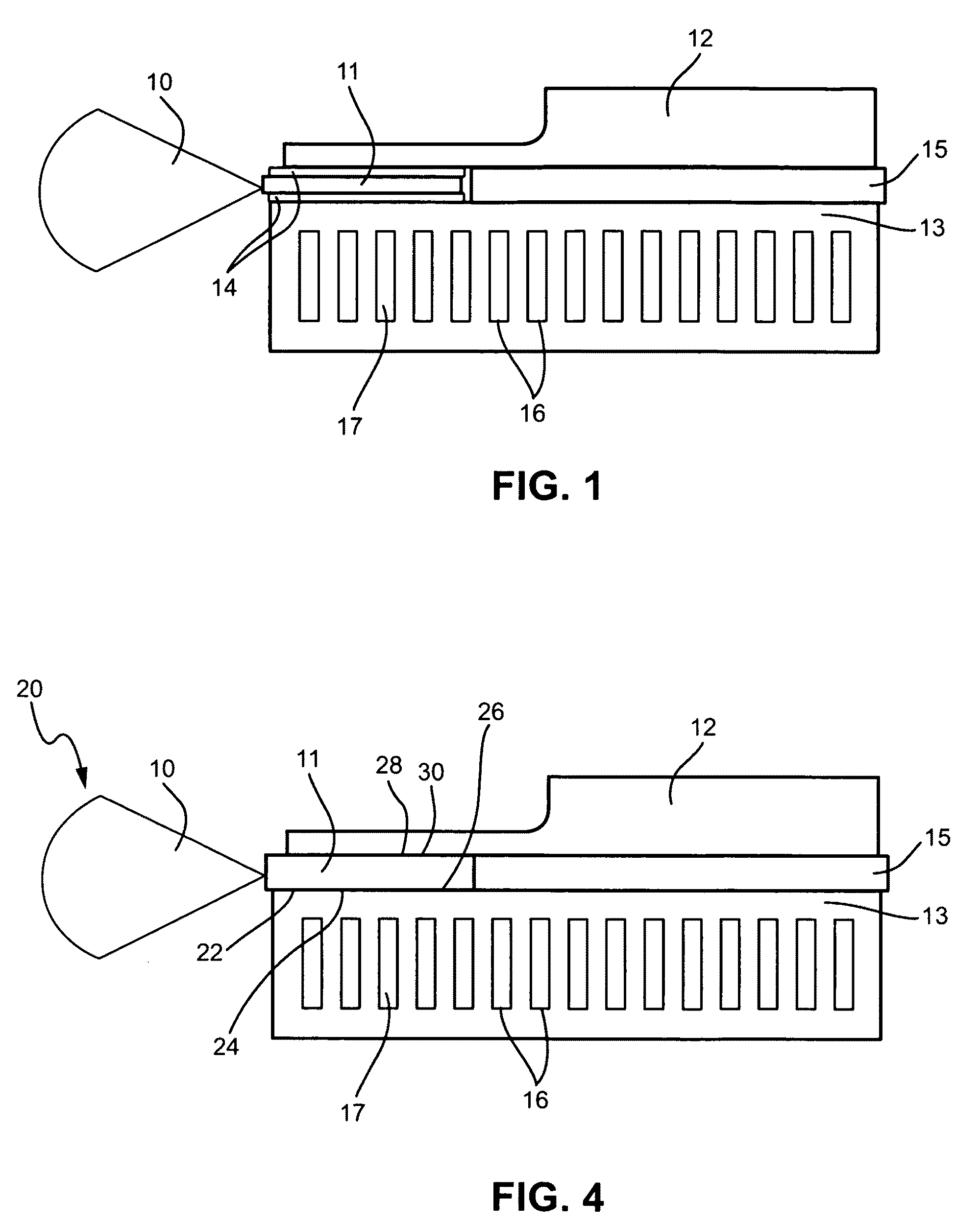
[0032]The present invention is directed to the implementation of laser diode systems in which one or more laser diode substrates are bonded to one or more metal substrates without the use of any intermediate soldering layer(s) between the two substrates. The presently described invention can be used for device fabrication, as well as for packaging of devices, and is very useful for many applications since it provides a lower thermal resistance across heterogeneous material interfaces. It also provides a low electrical resistance across a metal to semiconductor interface. Furthermore, this invention reduces fabrication and packaging complexity, as well as cost for a large and increasing number of photonic devices and systems.

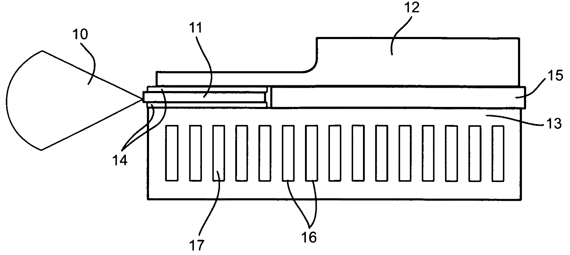
[0033]FIG. 1 is an illustration of a currently used implementation of laser diode systems in which the laser diodes are currently adjoined to metal substrates using a solder as an intermediate layer between the substrates. The intermediate material typically used...


PUM


Abstract

A laser diode system is disclosed in which a substrate made of a semiconductor material containing laser diodes is bonded to a substrate made from a metallic material without the use of any intermediate joining or soldering layers between the two substrates. The metal substrate acts as an electrode and/or heat sink for the laser diode semiconductor substrate. Microchannels may be included in the metal substrate to allow coolant fluid to pass through, thereby facilitating the removal of heat from the laser diode substrate. A second metal substrate including cooling fluid microchannels may also be bonded to the laser diode substrate to provide greater heat transfer from the laser diode substrate. The bonding of the substrates at low temperatures, combined with modifications to the substrate surfaces, enables the realization of a low electrical resistance interface and a low thermal resistance interface between the bonded substrates.

Description

CROSS-REFERENCES TO RELATED APPLICATIONS[0001]This application claims the benefit of Provisional Application No. 60 / 974,204, filed Sep. 21, 2007, and Provisional Application No. 61 / 034,611, filed Mar. 7, 2008, the entire contents of which are hereby incorporated by reference in this application.FIELD OF INVENTION[0002]The present invention relates to an improved implementation for systems containing laser diodes and laser diode arrays, involving the bonding of a substrate containing one or more solid-state laser diodes to another substrate made of a metal, or metal alloy. In addition, the present invention is applicable to other electronic fields including integrated circuits and MIMICs.BACKGROUND OF THE INVENTION[0003]The implementation of laser diodes systems for most applications involves the joining together of a semiconductor substrate containing the laser diode(s) or a laser diode arrays to a metallic substrate. This implementation approach has always involved the use of an in...

Claims


Application Information

Patent Timeline
IPC IPC(8): H01S5/024H01L21/77
CPCH01S5/02264H01S5/024H01S5/02423H01S5/02484H01S5/4025H01L2224/83192H01L2924/1461H01S5/02256H01S5/0425H01L2924/00H01S5/02345H01S5/02355H01S5/02365H01S5/0237
Inventor HUFF, MICHAEL A.JACOB, JONAH
Owner HUFF MICHAEL
Why Eureka
Try Eureka