Method for non-destructive patterning of photonic crystals employed for solid-state light extraction

a technology of photonic crystals and solid-state light extraction, applied in photomechanical equipment, instruments, manufacturing tools, etc., can solve the problems of requiring the use of expensive and time-consuming vacuum equipment (deposition, etching, lithography tools, etc., and achieve the effect of improving light extraction and being easily adaptabl

Inactive Publication Date: 2009-04-16
RGT UNIV OF CALIFORNIA
View PDF1 Cites 9 Cited by
  • Summary
  • Abstract
  • Description
  • Claims
  • Application Information

AI Technical Summary

Benefits of technology

[0023]The methodology of the present invention deals with a soft-lithography technique for the fabrication of sol-gel derived TiO2 photonic crystals for improved light extraction, thereby taking the NIL approach one step further. The liquid TiO2 precursor sol-gel is molded directly using an elastomeric soft stamp, based on thiol-ene curable polysiloxane, which is described in the cross-referenced application by the inventors of the present invention,6 and partially cured at low temperature until the pattern is transferred and the mold can be removed. The only subsequent processing necessary is calcination at a desired temperature suitable for the specific application, typically between 200° C. and 700° C. This nano-fabrication method is fast, cheap, can be scaled up, and does not require any vacuum deposition or additional etching. In addition, sol-gel chemistry is very versatile and can be easily adapted to a variety of different materials and applications (e.g. mixed and doped metal-oxides, incorporation of nano-particles).

Problems solved by technology

Unconventional methods for nano-fabrication (i.e. molding, embossing, printing, self-assembly etc.) offer a low-cost alternative to conventional lithography and etching techniques, which often lead to substantial damage of the underlying optical active area and / or conductive layers and require the use of expensive and time consuming vacuum equipment (deposition, etching) and lithography tools (e.g. photolithography, scanning beam lithography).5 Nano-imprint lithography (NIL) uses a rigid mold for pressure-induced pattern transfer into a thermoplastic polymer film, which serves as an etch mask to transfer the pattern into an underlying substrate.
However, this technique still relies on hard molds, which tend to wear during thermal cycling and pressure and also require expensive reactive ion etching (RIE) or inductively coupled plasma (ICP) etch steps.
However, doing holographic lithography on each sample is time consuming and not viable for industry.
With the former approach, nano-scale feature sizes can be realized, but the writing process is a conventional e-beam process and inherently too slow and expensive for mass-production.
The second approach is not really suitable for nano-scale features, even with the use of extremely expensive optical equipment.
These techniques, also more broadly known as ‘soft lithography,’ have successfully been demonstrated for dimensions in the micrometer scale but have been shown to fail for smaller feature sizes and high aspect ratios.
In addition, swelling of the mold in a variety of solvents limits the life-time of the mold, which is not sufficient for industrial use yet.
Another issue associated with this technique is that it is nearly impossible to completely de-wet the surface between the mold and the substrate, and a small residual scum layer of the molded material is likely to be present.
WO05101466A2, but a commercially viable process for mass-production has not been established yet.
Spin-on based titanium dioxide nano-structures have recently been fabricated in combination with holographic lithography.17 A significant drawback of the holographic techniques is the sinusoidal shape inherent to the interference pattern, which does not allow for high aspect ratios and leads to less sharply defined features.

Method used


Image

  • Method for non-destructive patterning of photonic crystals employed for solid-state light extraction
  • Method for non-destructive patterning of photonic crystals employed for solid-state light extraction
  • Method for non-destructive patterning of photonic crystals employed for solid-state light extraction

Examples


Embodiment Construction

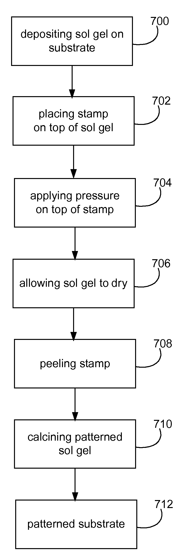
[0035]In the following description of the preferred embodiment, reference is made to the accompanying drawings which form a part hereof, and in which is shown by way of illustration a specific embodiment in which the invention may be practiced. It is to be understood that other embodiments may be utilized and structural changes may be made without departing from the scope of the present invention.

[0036]Overview

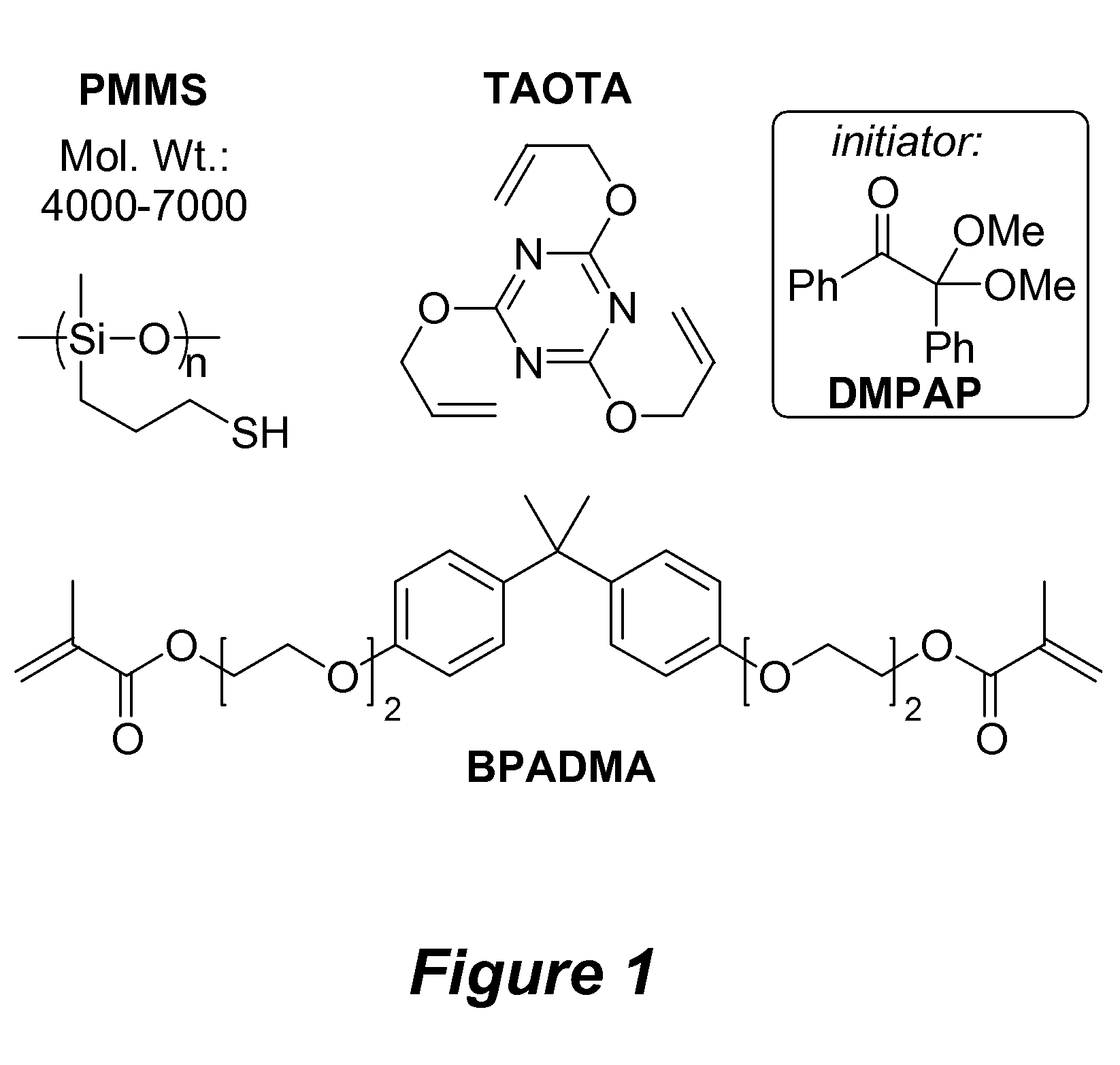
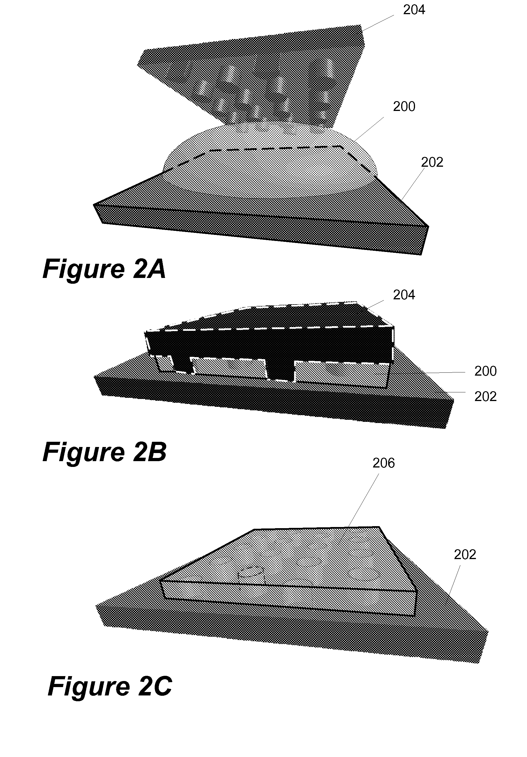
[0037]Photonic crystals have been suggested to increase the light extraction out of inorganic (see U.S. Pat. No. 5,955,749) or organic LEDs (see U.S. Pat. No. 6,630,684 B2), and high and low refractive index materials, e.g. titanium dioxide, zirconia or silica, play an important role in order to achieve periodic structures with high refractive index contrast. Efficient and inexpensive patterning methods with high reproducibility are important for mass-production of such devices. The most commonly used method in micro-electronics is photolithography, where a predetermined patte...


PUM

PropertyMeasurementUnit
pressureaaaaaaaaaa
pressureaaaaaaaaaa
feature sizesaaaaaaaaaa

Abstract

A method for patterning metal oxides or ceramics on surfaces, and more particularly, a method of forming photonic crystals. The patterning is done using a solution coating process and a polymer-based template made by nano-imprint lithography. The methodology to pattern a sol-gel can be used to make features without the undesired scum layer. Furthermore, the patterned photonic crystals were demonstrated to efficiently increase the light extraction efficiency of solid state devices based on GaN.

Description

CROSS REFERENCE TO RELATED APPLICATIONS[0001]This application claims the benefit under 35 U.S.C. Section 119(e) of co-pending and commonly-assigned U.S. Provisional Patent Application Ser. No. 60 / 979,759, filed on Oct. 12, 2007, by Luis M. Campos, Craig J. Hawker, and Ines Meinel, entitled “METHOD FOR NON-DESTRUCTIVE PATTERNING OF PHOTONIC CRYSTALS EMPLOYED FOR SOLID-STATE LIGHT EXTRACTION,” attorney's docket number 30794.252-US-P1 (2008-054), which application is incorporated by reference herein.[0002]This application is related to the following co-pending and commonly-assigned U.S. patent applications:[0003]U.S. Utility application Ser. No. ______, filed on same date herewith, by Craig J. Hawker, Luis M. Campos and Ines Meinel, entitled “THIOL-ENE BASED POLY(ALKYLSILOXANE) MATERIALS,” attorney's docket number 30794.251-US-U1 (2008-055), which application claims the benefit under 35 U.S.C. Section 119(e) of co-pending and commonly-assigned U.S. Provisional Application Ser. No. 60 / 9...

Claims


Application Information

Patent Timeline
Patent Type & Authority Applications(United States)
IPC IPC(8): B29C41/42B32B3/00
CPCB82Y10/00Y10T428/24479G03F7/0002B82Y40/00
Inventor CAMPOS, LUIS M.HAWKER, CRAIG J.MEINEL, INES
Owner RGT UNIV OF CALIFORNIA
Why Eureka
Try Eureka