Epitaxial methods and templates grown by the methods

Active Publication Date: 2009-04-16
S O I TEC SILICON ON INSULATOR THECHNOLOGIES +1
View PDF83 Cites 66 Cited by
  • Summary
  • Abstract
  • Description
  • Claims
  • Application Information

AI Technical Summary

Benefits of technology

[0035]In the case of applications to III nitrides, the term “reduced levels of lattice strain” refers herein to a level of strain, for a given composition, that is less than the level of strain present at the critical thickness for the formation of crystal defects during hetero-epitaxial growth. To further explain, a limited amount of elastic strain can be accommodated by a material without generating dislocations or defects. This accommodation requires an amount of energy which is governed by the material thickness and size of the lattice mismatch. Energy is also required to create a defect in the material to relieve the lattice strain. If the strain is greater t

Problems solved by technology

However, this trade name should not be interpreted restrictively, be

Method used


Image

  • Epitaxial methods and templates grown by the methods
  • Epitaxial methods and templates grown by the methods
  • Epitaxial methods and templates grown by the methods

Examples


example 1

[0127]FIGS. 7A-B illustrate top views and FIG. 7C illustrates a TEM side view of an actual examples of a preferred base substrate 111 with a plurality GaN islands / pillars, in particular islands / pillar 103, 105, and 107, corresponding to the schematic illustration in FIG. 4B. The double headed arrow in FIG. 7A represent 100 μm and in FIG. 7B represents 50 μm. FIG. 7B illustrates in more detail the region of FIG. 7A within frame 101.

[0128]The island / pillar features of FIGS. 7A-C have been produced by heating a MOVPE reactor to temperature of between 800° C. to 1000° C., in preferred embodiment the temperature was maintained at 900° C. during the growth of the isolated GaN features. The pressure range during the growth was maintained between 200 Torr to 400 Torr, in preferred embodiment the pressure was maintained at 200 Torr. The ratio of V species (e.g. Ammonia) to III species (e.g. Trimethylgallium) was kept low to promote 3-D pillar growth; V / III ratios utilized were between 700-12...

example 2

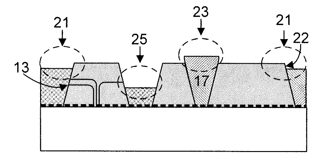
[0134]FIG. 8 illustrates an alternative embodiment for producing substantially isolated pillars / islands of a III nitride material. The GaN islands illustrated in FIG. 8 were produced by the etching of a 2D layer of III nitride material that included regions with significantly different etch resistance. The etch resistance across a III nitride layer can vary substantially depending on the crystal polarity and / or defect density in a particular area, for example growth conditions are known in the art which can lead to GaN layers with varying crystal polarity across a wafer. The etch conditions for the example shown in FIG. 8 involved the exposure of a substantially continuous GaN film to a potassium hydroxide etch solution at a temperature of 80° C. for a time period of between 6-10 minutes.

[0135]The resulting pillar / island-like features are generally spatially separated, with the underlying substrate exposed between the features, have a generally uniform maximum height, and a truncate...


PUM


Abstract

This invention provides methods for fabricating substantially continuous layers of a group III nitride semiconductor material having low defect densities and optionally having a selected crystal polarity. The methods include epitaxial growth nucleating and/or seeding on the upper portions of a plurality of pillars/islands of a group III nitride material that are irregularly arranged on a template structure. The upper portions of the islands have low defect densities and optionally have a selected crystal polarity. The invention also includes template structures having a substantially continuous layer of a masking material through which emerge upper portions of the pillars/islands. The invention also includes such template structures. The invention can be applied to a wide range of semiconductor materials, both elemental semiconductors, e.g., combinations of Si (silicon) with strained Si (sSi) and/or Ge (germanium), and compound semiconductors, e.g., group II-VI and group III-V compound semiconductor materials.

Description

CROSS-REFERENCE TO RELATED APPLICATIONS[0001]This application claims the benefit of U.S. Provisional Application No. 60 / 952,131 filed Jul. 26, 2007, which is included by reference herein in its entirety for all purposes.FIELD OF THE INVENTION[0002]The present invention relates to the field of processing semiconductor materials, and in particular to the field of epitaxial growth of high-quality, mono-crystalline layers of semiconductor materials. The invention provides epitaxial methods which, in preferred embodiments, combine damascene techniques with epitaxial lateral overgrowth (ELO) techniques. The invention also provides templates and semiconductors fabricated by the provided Damascene-ELO™ methods.BACKGROUND OF THE INVENTION[0003]To be suitable for device fabrication, layers of semiconductor materials must be of high purity and have low densities of defects or dislocations. Preparation of quality layers of certain materials, especially compound materials, has been hindered in t...

Claims


Application Information

Patent Timeline
IPC IPC(8): H01L21/20B32B3/10
CPCH01L21/02645H01L21/02647H01L21/0254H01L21/02458Y10T428/24612H01L21/02639H01L21/0237H01L21/02642
Inventor ARENA, CHANTALWERKHOVEN, CHRISTIAAN J.BERTRAM, JR., RONALD THOMASLIDOW, EDMAHAJAN, SUBHASHDATTA, RANJANTRIVEDI, RAHUL AJAYHAN, ILSU
Owner S O I TEC SILICON ON INSULATOR THECHNOLOGIES
Why Eureka
Try Eureka