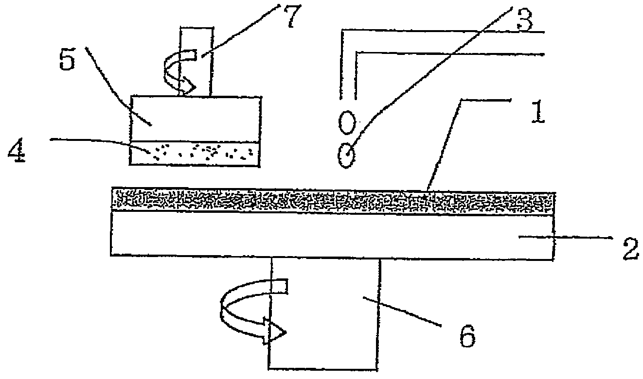
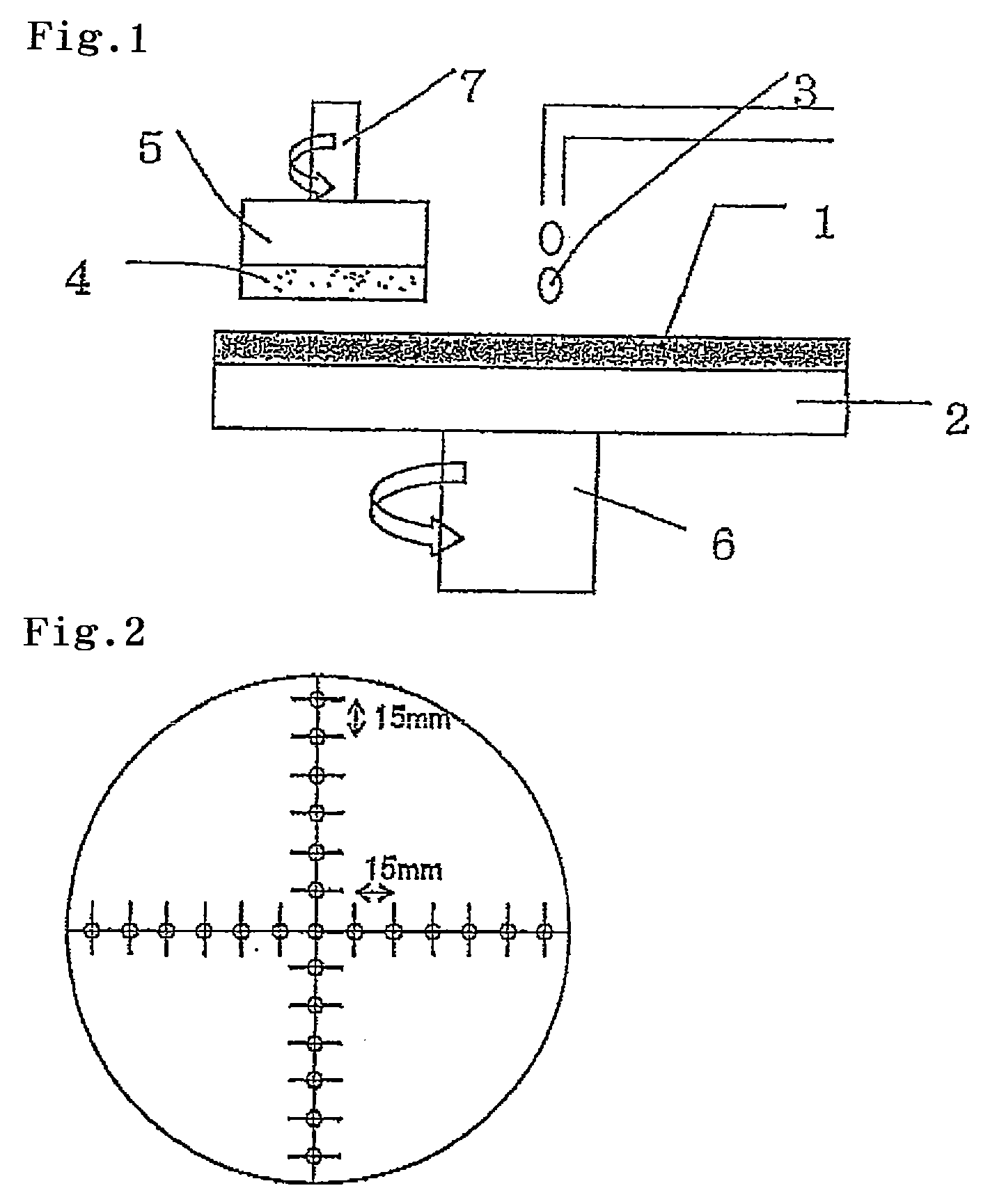
Polishing pad

a technology of polishing pad and polishing surface, which is applied in the field of polishing pad, can solve the problems of unreacted polyol component remaining in the material, deteriorating inability to obtain uniform physical properties of the polishing pad, etc., and achieves superior longevity and excellent polishing rate.

Active Publication Date: 2009-04-23
ROHM & HAAS ELECTRONICS MATERIALS CMP HLDG INC
View PDF42 Cites 17 Cited by
  • Summary
  • Abstract
  • Description
  • Claims
  • Application Information

AI Technical Summary

Benefits of technology

[0011]An object of the present invention is to provide a polishing pad excellent in polishing rate and superior in longevity without generating center slow. Another object of the present invention is to provide a method of manufacturing a semiconductor device with the polishing pad.

Problems solved by technology

In the method (1), however, there is a possibility that when the matrix material is polyurethane, active hydrogen-containing hydrophilic groups such as hydroxyl groups react with isocyanate groups in synthesis of polyurethane, and as a result, an unreacted polyol component remains in the material.
This remaining polyol component gives rise to a plasticizing effect so that the physical properties of the polishing pad tend to be deteriorated.
In the method (2), the hydrophilic substance is hardly uniformly mixed in the matrix material, so a polishing pad having uniform physical properties cannot be obtained.
When the polishing rate varies from the start of use to the end of use, the polishing conditions should be regulated, and there is also the problem of poor efficiency of polishing.
However, the polishing material disclosed in Patent Literature 5 consists of non-foam urethane, and the non-foam polishing material is provided with grooves because of low polishing rate, but abrasive grains and polishing waste etc. in slurry are topically present etc. to make the stabilization of the polishing rate very difficult.
The polishing cloth disclosed in Patent Literature 6 is easily worn, is poor in hardness (due to uneven cells and large cell diameters), and is thus poor in planarity and uniformity, and the polishing rate is inevitably changed significantly.
Further, the conventional polishing pad has a problem of center slow (phenomenon where the center of a wafer is hardly polished).

Method used


Image

  • Polishing pad
  • Polishing pad

Examples


example 1

[0091]350 parts by weight of polytetramethylene glycol (PTMG with a number-average molecular weight of 650, manufactured by Mitsubishi Chemical Corporation) and 57 parts by weight of diethylene glycol (DEG, manufactured by Mitsubishi Chemical Corporation) were introduced into a separable flask, and dehydrated under stirring under reduced pressure for 2 hours. By introducing nitrogen into the separable flask, the atmosphere therein was replaced by nitrogen, and 300 parts by weight of toluene diisocyanate (a mixture of 2,4-diisocyanate / 2,6-diisocyanate in a ratio of 80 / 20 manufactured by Mitsui Takeda Chemicals, Inc.; hereinafter referred to as TDI-80) and 114 parts by weight of 4,4′-dicyclohexyl methane diisocyanate (hereinafter abbreviated as HMDI) were added thereto. While the temperature of the reaction system was kept at about 70° C., the reaction mixture was stirred until the reaction was finished. The reaction was regarded to be finished when NCO % became almost constant (NCO %...

example 2

[0095]1113 parts by weight of polytetramethylene glycol (PTMG with a number-average molecular weight of 1000, manufactured by Mitsubishi Chemical Corporation), 196 parts by weight of polytetramethylene glycol (PTMG with a number-average molecular weight of 650, manufactured by Mitsubishi Chemical Corporation) and 150 parts by weight of diethylene glycol (DEG, manufactured by Mitsubishi Chemical Corporation) were introduced into a separable flask, and dehydrated under stirring under reduced pressure for 2 hours. By introducing nitrogen into the separable flask, the atmosphere therein was replaced by nitrogen, and 900 parts by weight of TDI-80 and 151 parts by weight of HMDI were added thereto. While the temperature of the reaction system was kept at about 70° C., the reaction mixture was stirred until the reaction was finished. The reaction was regarded to be finished when NCO % became almost constant (NCO %=9.1). Thereafter, the reaction solution was defoamed under reduced pressure ...

example 3

[0097]A polishing pad was prepared in the same manner as in Example 1 except that 25.2 parts by weight of ETACURE 300 (a mixture of 3,5-bis(methylthio)-2,6-toluene diamine and 3,5-bis(methylthio)-2,4-toluene diamine), manufactured by Albemarle Corporation) were used in place of 28.7 parts by weight of MOCA.


PUM

PropertyMeasurementUnit
specific gravityaaaaaaaaaa
tensile strengthaaaaaaaaaa
tensile elongation at breakaaaaaaaaaa

Abstract

An object of the present invention is to provide a polishing pad excellent in polishing rate and superior in longevity without generating center slow. Another object of the present invention is to provide a method of manufacturing a semiconductor device with the polishing pad. Disclosed is a polishing pad having a polishing layer consisting of a polyurethane foam having fine cells, wherein a high-molecular-weight polyol component that is a starting component of the polyurethane foam contains a hydrophobic high-molecular-weight polyol A having a number-average molecular weight of 550 to 800 and a hydrophobic high-molecular-weight polyol B having a number-average molecular weight of 950 to 1300 in an A/B ratio of from 10/90 to 50/50 by weight.

Description

TECHNICAL FIELD[0001]The invention relates to a polishing pad capable of performing planarization of materials requiring a high surface planarity such as optical materials including a lens and a reflecting mirror, a silicon wafer, a glass substrate or an aluminum substrates for a hard disc and a product of general metal polishing with stability and a high polishing efficiency. A polishing pad of the invention is preferably employed, especially, in a planarization step of a silicon wafer or a device on which an oxide layer or a metal layer has been formed prior to further stacking an oxide layer or a metal layer thereon.BACKGROUND ART[0002]Typical materials requiring surface flatness at high level include a single-crystal silicon disk called a silicon wafer for producing semiconductor integrated circuits (IC, LSI). The surface of the silicon wafer should be flattened highly accurately in a process of producing IC. LSI etc., in order to provide reliable semiconductor connections for v...

Claims


Application Information

Patent Timeline
Patent Type & Authority Applications(United States)
IPC IPC(8): B24B1/00B24B7/20B24B37/20B24B37/24C08G18/65H01L21/304
CPCB24B37/24B24D3/32Y10T428/24C08G2101/00C08G18/36Y10T428/249953C08G18/65H01L21/304
Inventor OGAWA, KAZUYUKISHIMOMURA, TETSUONAKAI, YOSHIYUKINAKAMORI, MASAHIKOYAMADA, TAKATOSHI
Owner ROHM & HAAS ELECTRONICS MATERIALS CMP HLDG INC
Why Eureka
Try Eureka