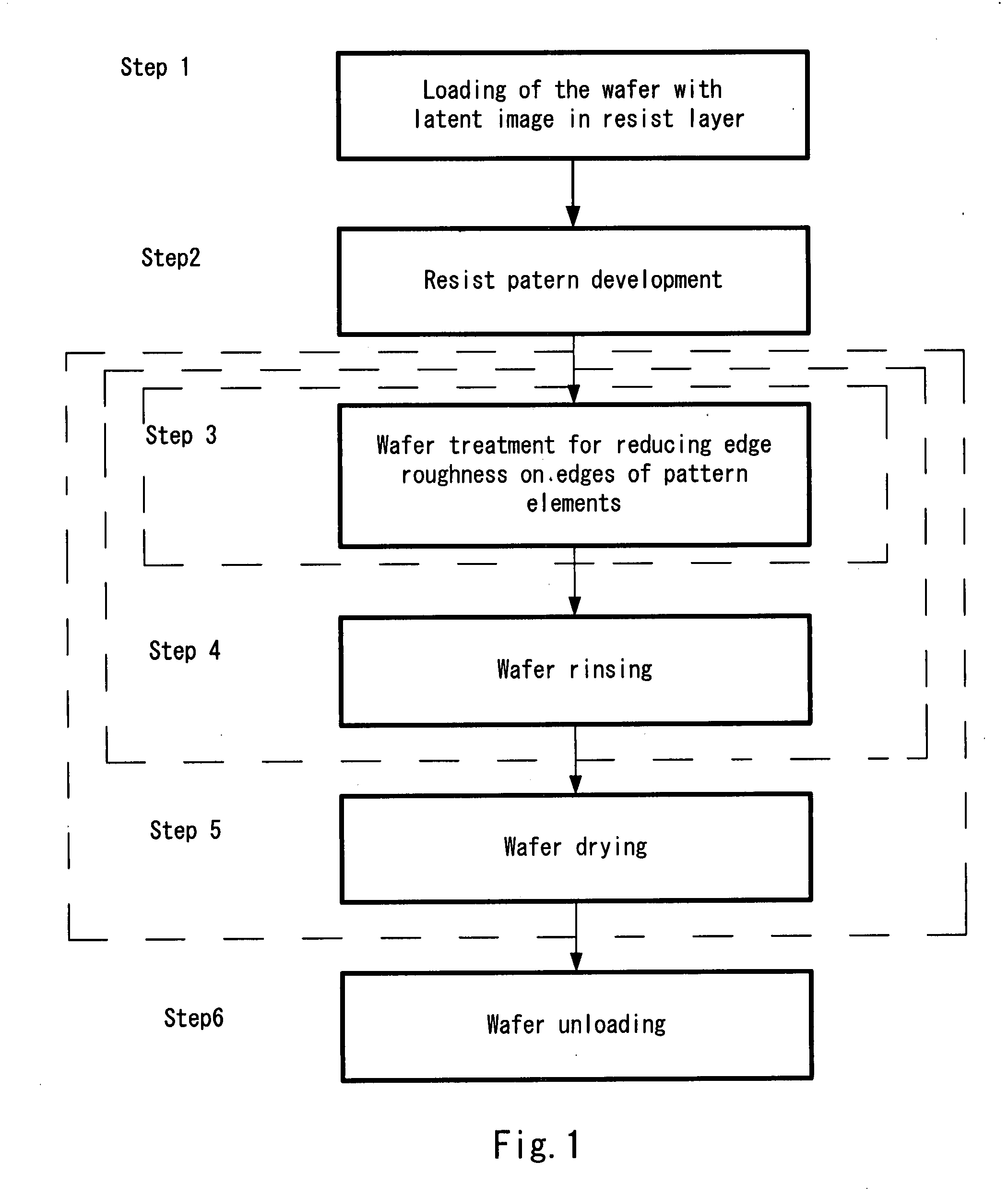
[0018]It is an object of the present invention to provide a method and an apparatus for smoothening rough edges of lithographic patterns by
softening the material of the edges to a degree that allows smoothening under effect of
surface tension. It is another object to provide a method and apparatus which make it possible to improve quality of the pattern elements without deviations from the designed dimensions. It is another object to provide a LER reduction to a very fine degree of smoothening without deviations from the desired contours and designed dimensions of the pattern lines. A further object is to provide a process that is not subject to segregation effects, does not involve a large amount of chemicals, is easy to control, is versatile, has sufficient flexibility, and is not associated with the formation of liquid films known to induce mechanical pattern damage. It is another object of the invention to provide the aforementioned method and apparatus that do not need the use of vacuum and associated complicated equipment. It is a further object to provide an apparatus in which LER treatment, rinsing, and
drying are carried out in a single working chamber.
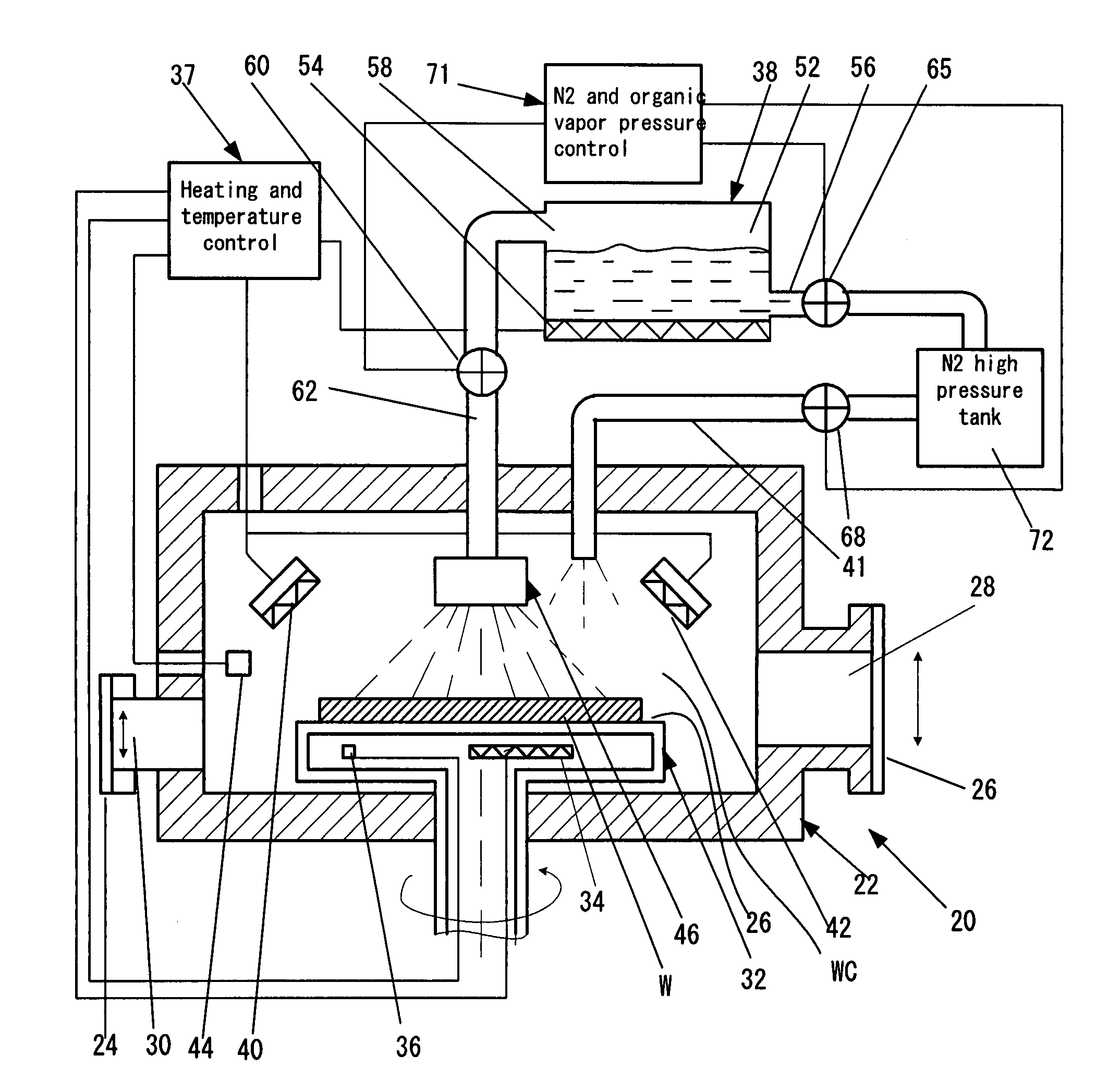
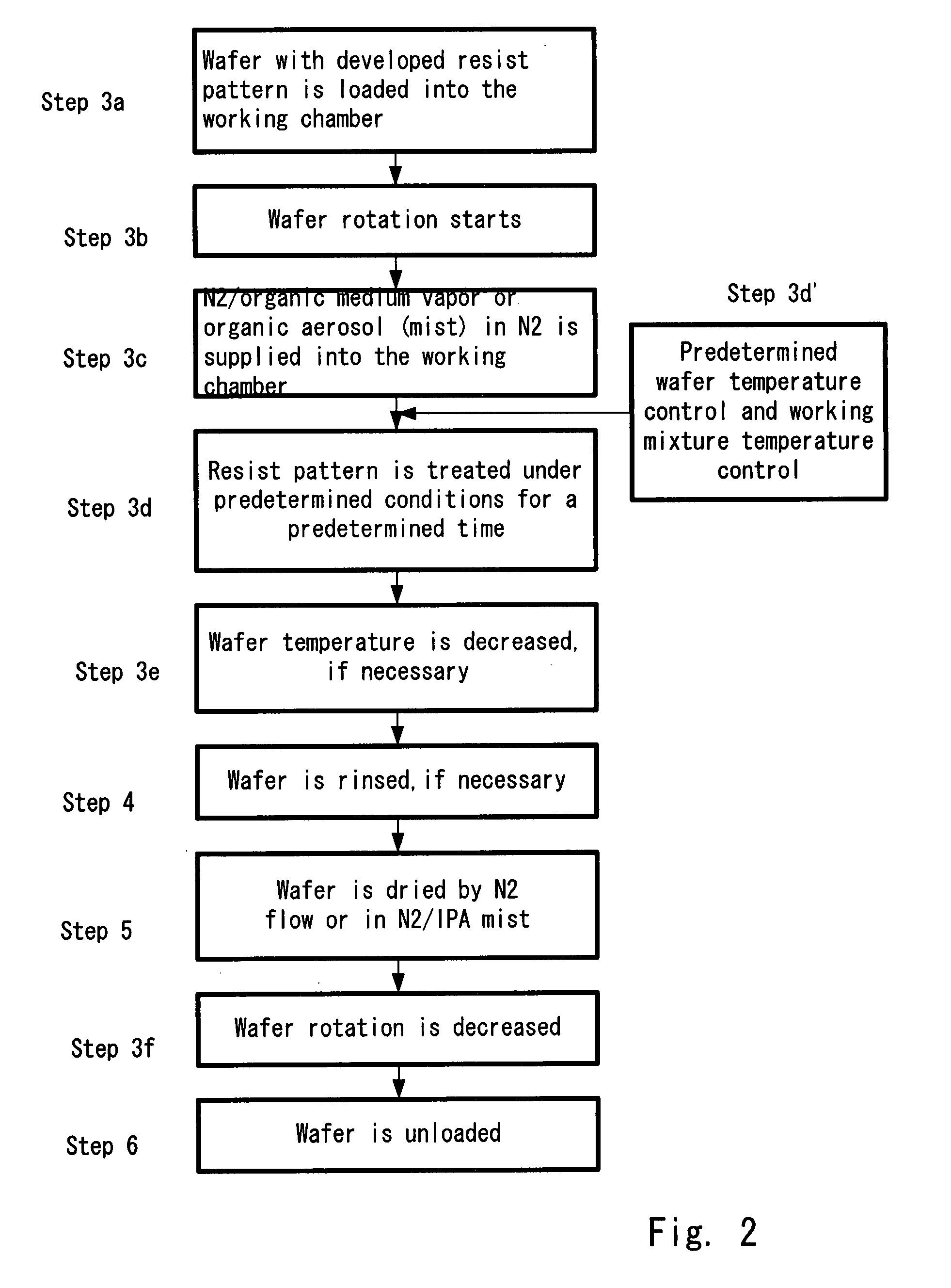
[0019]The proposed concept utilizes post develop / rinse
wafer treatment with gaseous mixture consisting of neutral carrier gas (such as
nitrogen,
argon) saturated with
resist solvent vapors, or in another embodiment with fine
aerosol. If the temperature of the
wafer surface is maintained slightly higher (by about 3-10° C.) than the treating gaseous mix, then the
solvent does not condense over the surface forming a liquid film, allowing treatment without having liquid film over the surface. This is the major
advantage as compared with the existing methods since the method of the invention utilizes the effect of surface tension for smoothening nano-roughnesses formed on the surfaces of the microelements after conventional microlithographic processes. According to the invention, the pattern is treated under normal pressure in the
atmosphere of a phase of the aforementioned organic substance selected from vapor of an
organic vapor or mist of organic substance in
nitrogen or another gas. Two
modes are possible: 1) direct
diffusion of
organic molecules into the
surface layer of the pattern material; or 2) condensation onto the pattern surface with the formation of an extremely thin
organic film, which also leads to diffusion of the organic molecules into the pattern material.
Solvent molecules, being dissolved in the upper pattern layer, provide mobility to the surface molecules assisting surface in its natural tendency to minimize
surface energy by minimizing the surface area.
Solid materials cannot undergo surface minimization due to rigidity, and are therefore characterized by high levels of
surface energy. On the other hand,
solvent molecules, which are dissolved in-between the
polymer molecules, increase their mobility, while
surface energy minimization drives
polymer molecules to move from high points to low ones thus
smoothing the surface. The solvent
dissolution levels are also higher for the
high surface topography spots additionally assisting their faster
smoothing. Once the surface is smoothened to the required roughness, the treatment is switched to
inert gas only (at the similar conditions) and assists in
evaporation of the dissolved solvent.
[0022]The process may be carried out at
atmospheric pressure or at a slightly higher pressure such as normally used in the
lithography tracks to prevent penetration of the external ambient gases into the treatment chamber. The process temperature is normally close to the solvent boiling points (BP). For the
aerosol or mist version the temperature could be slightly lower than the BP to prevent
aerosol evaporation, and for the vapor-carrier gas mix it could be slightly higher than the BP, to prevent vapor condensation.

