

Manufacturing method of a semiconductor device
- Summary
- Abstract
- Description
- Claims
- Application Information
AI Technical Summary
Benefits of technology
Problems solved by technology
Method used
Image

Examples
embodiment 1
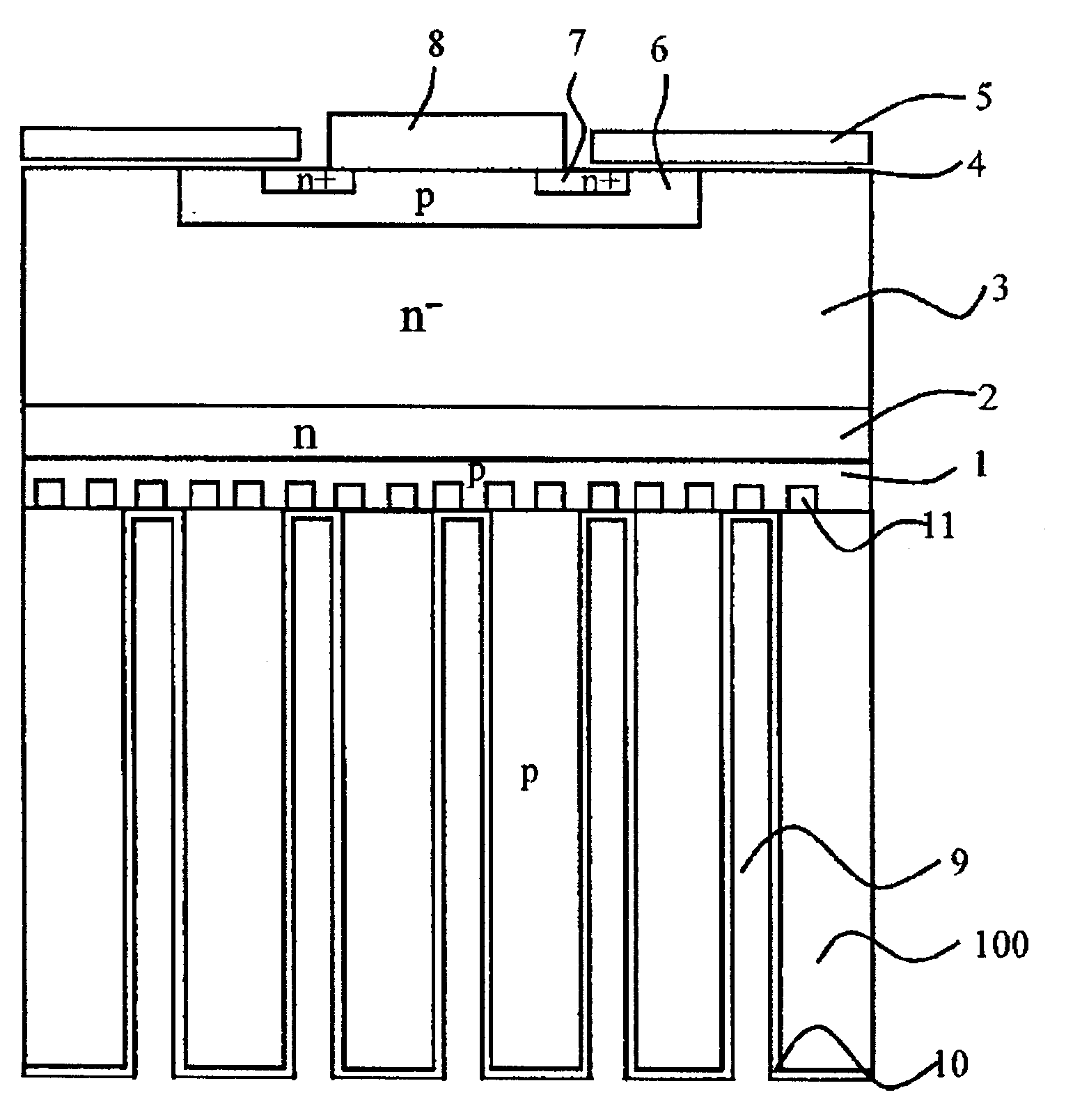
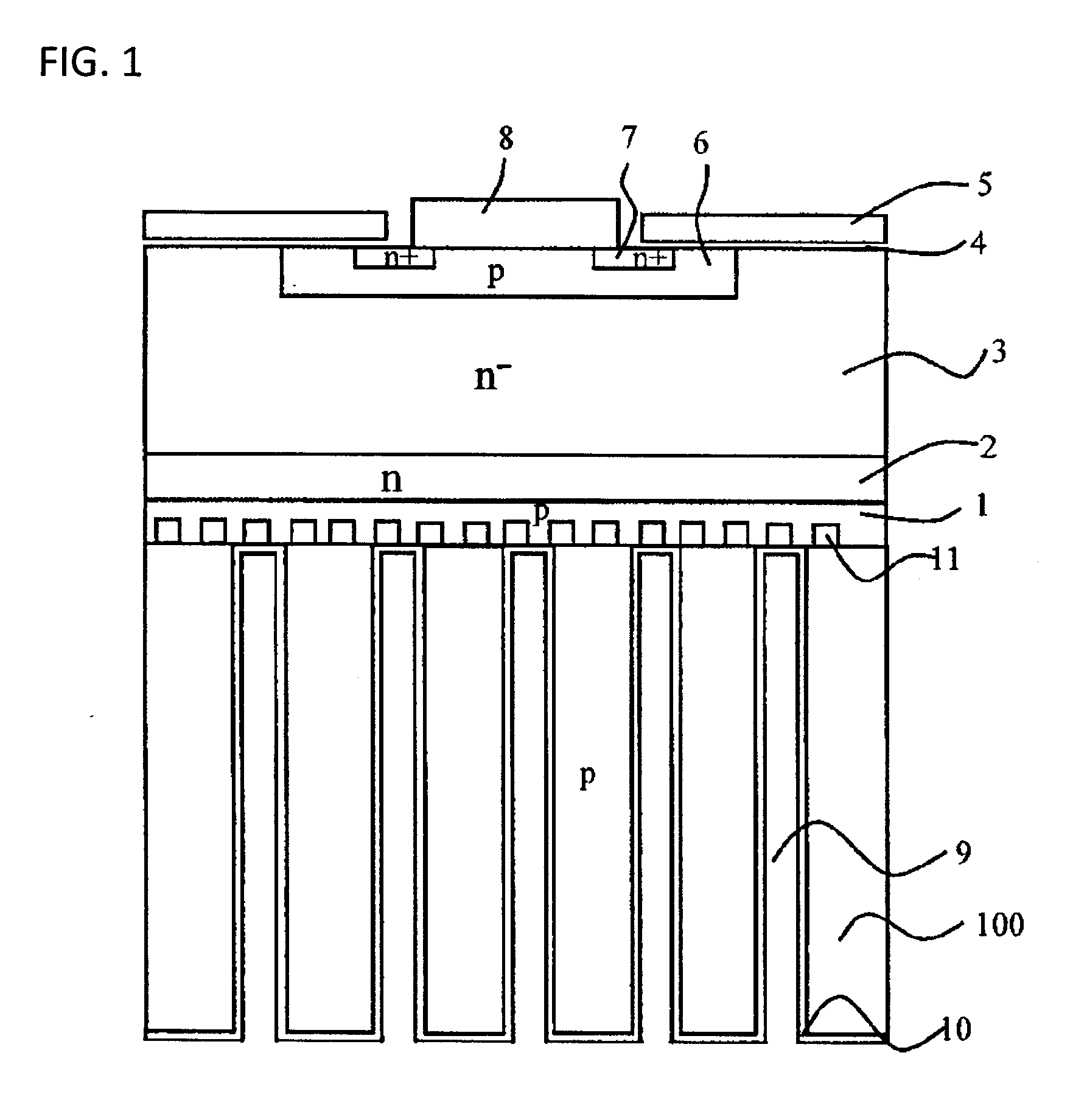
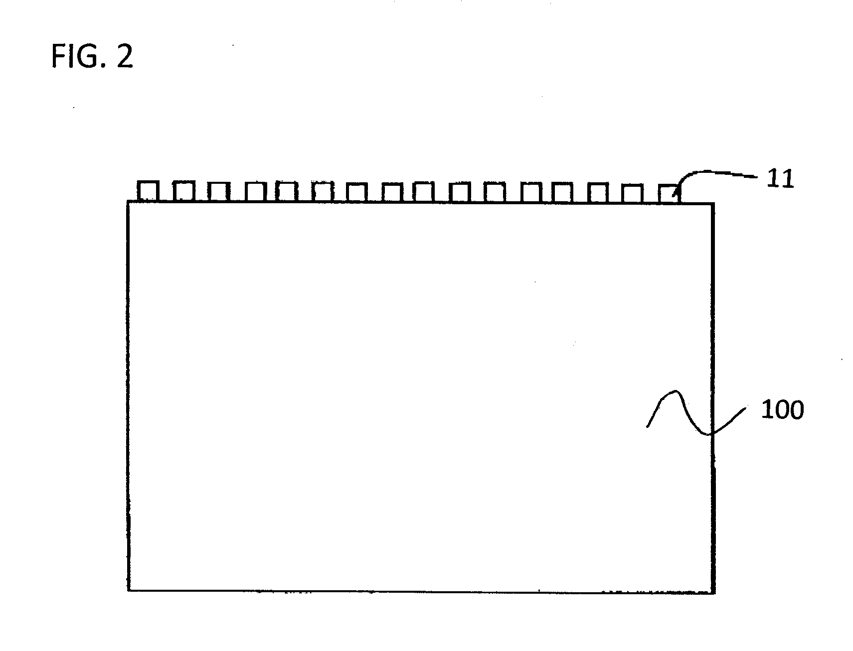
[0042]A first embodiment of the invention will be described below in detail with reference to FIGS. 1-6. The first embodiment is directed to an IGBT having a breakdown voltage of 600V. FIG. 1 is a sectional view of an important part of an IGBT according to the first embodiment. As shown in FIG. 1, in the IGBT according to the first embodiment, a silicon oxide film 11 is formed on a 500-μm-thick high-resistivity p-type silicon substrate 100 so as to have a selectively formed pattern. A 0.6-μm-thick epitaxial p-type layer (first semiconductor layer; may be hereinafter abbreviated as “p-type collector layer”) 1 having an impurity concentration of 3.0×1017 cm−3 and a 2.0-μm-thick epitaxial n-type layer (second semiconductor layer) 2 having an impurity concentration of 2.0×1016 cm−3 are formed on the silicon oxide film 11 by epitaxial silicon growth. An epitaxial high-resistivity n− drift layer (third semiconductor layer) 3 is laid on the epitaxial n-type layer 2. To attain a breakdown v...
embodiment 2
[0052]FIG. 7 is a sectional view of an important part of an IGBT having a breakdown voltage of 600 V according to a second embodiment. As shown in FIG. 7, in the IGBT according to the second embodiment, as in the IGBT according to the first embodiment, a silicon oxide film 11 is formed on an 8-inch-diameter high-resistivity p-type silicon substrate 100 so as to have a selectively formed pattern. A 0.6-μm-thick epitaxial p-type collector layer 1 having an impurity concentration of 3.0×1017 cm−3 and a 3.0-μm-thick epitaxial n-type layer 2 having an impurity concentration of 2.0×1016 cm−3 are formed on the silicon oxide film 11. An epitaxial high-resistivity n− drift layer 3 is laid on the epitaxial n-type layer 2. Although in the second embodiment the high-resistivity p-type silicon substrate 100 is used as a thick silicon substrate (support substrate), a high-resistivity n-type silicon substrate may be used instead. To attain a breakdown voltage of 600 V with a sufficient margin, as ...
embodiment 3
[0055]FIG. 9 is a sectional view of an important part of a MOSFET having a breakdown voltage of 600 V according to a third embodiment. As shown in FIG. 9, in the MOSFET according to the third embodiment, a silicon oxide film 11 is formed on a high-resistivity n-type silicon substrate 200 so as to have a selectively formed pattern. A 2.0-μm-thick epitaxial n-type layer 2 having an impurity concentration of 2.0×1019 cm−3 is formed on the silicon oxide film 11, and an epitaxial high-resistivity n− drift layer 3 is laid on the epitaxial n-type layer 2. To attain a breakdown voltage of 600 V with a sufficient margin, the impurity concentration and the thickness of the epitaxial high-resistivity n− drift layer 3 are set at 2.5×1014 cm−3 and 55 μm, respectively. Then, a 100-nm-thick gate oxide film 4 is formed and a gate electrode 5 is formed by forming and patterning a polysilicon layer. A p-type channel region 6 and n+ source regions 7 are formed by ion implantation and thermal diffusion...
PUM
 Abstract
Description
Claims
Application Information