Electromagnetic shielding film and optical filter

a technology of electromagnetic shielding film and optical filter, which is applied in the direction of optics, electrical equipment, instruments, etc., can solve the problems of unsuitable methods for shielding electromagnetic waves from display devices, unsuitable health disorders of operators of equipment, and inability to protect electromagnetic waves. , to achieve the effect of minimizing image quality deterioration, excellent electromagnetic shielding property and light transmittan

Active Publication Date: 2009-05-21
FUJIFILM CORP
View PDF15 Cites 33 Cited by
  • Summary
  • Abstract
  • Description
  • Claims
  • Application Information

AI Technical Summary

Benefits of technology

[0046]As described above, the electromagnetic shielding film and the optical filter of the present invention are excellent in the electromagnetic shielding property and light transmittance, and capable of minimizing image quality deterioration due to the moire or the like.

Problems solved by technology

It has been indicated that the EMI causes malfunction or failure of the electronic or electric equipment, and further causes health disorder of an operator of the equipment.
However, in the case of using the above methods, the front surface of the display device is likely to be opaque.
Thus, the methods are unsuitable for shielding the electromagnetic wave from the display devices.
However, a moire is often generated due to interference between the film material and a pixel pattern of the PDP.
However, this method is disadvantageous in complicated production process and in high cost.
Further, these methods are poor in wire resolution.
Thus, in these methods, the mesh pattern has a large wire width of 20 to 30 μm, so that the moire cannot be sufficiently reduced.
However, a large number of suitable films are needed for the PDP pixel patterns, whereby this method is disadvantageous in increased cost and storage.
Though the moire can be effectively reduced by thinning the wire of the mesh pattern, the thinning results in surface resistance increase and complicated production process disadvantageously.

Method used


Image

  • Electromagnetic shielding film and optical filter
  • Electromagnetic shielding film and optical filter
  • Electromagnetic shielding film and optical filter

Examples


first example

[0303]The present invention will be described more specifically below with reference to Examples. Materials, amounts, ratios, treatment contents, treatment procedures, and the like, used in Examples, may be changed without departing from the scope of the invention. The following examples are, therefore, to be considered in all respects as illustrative and not restrictive.

(Photosensitive Silver Halide Material)

[0304]An emulsion, which contained an aqueous medium, a gelatin, and silver iodobromochloride particles (I content: 0.2 mol %, Br content: 40 mol %, average spherical equivalent diameter: 0.1 μm), was prepared. The amount of the gelatin was 10.0 g per 60 g of Ag.

[0305]K3Rh2Br9 and K2IrCl6 were added to the emulsion at a concentration of 10−7 mol / mol silver to dope the silver bromide particles with Rh and Ir ions. Further, Na2PdCl4 was added to the emulsion, and the resultant emulsion was gold-sulfur-sensitized using chlorauric acid and sodium thiosulfate. The obtained emulsion ...

second example

[0323]Films of Examples 1 to 21 and Comparative Examples 1 to 3 were produced and the moire, conductivity, and light transmittance of each film were evaluated in the same manner as First Example. The conditions and the evaluation results of Examples 1 to 21 and Comparative Examples 1 to 3 are shown in Table 2.

examples 1 to 21

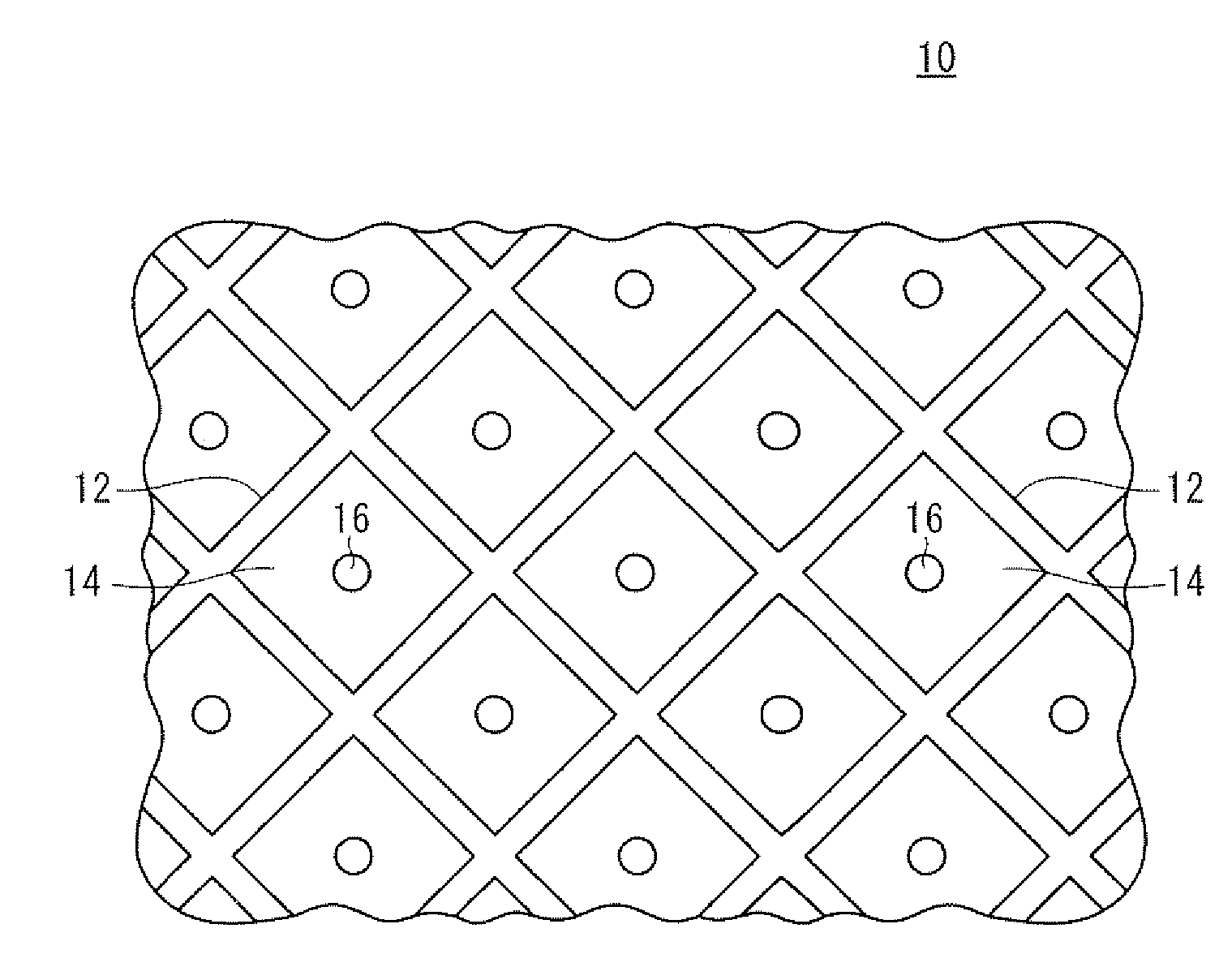
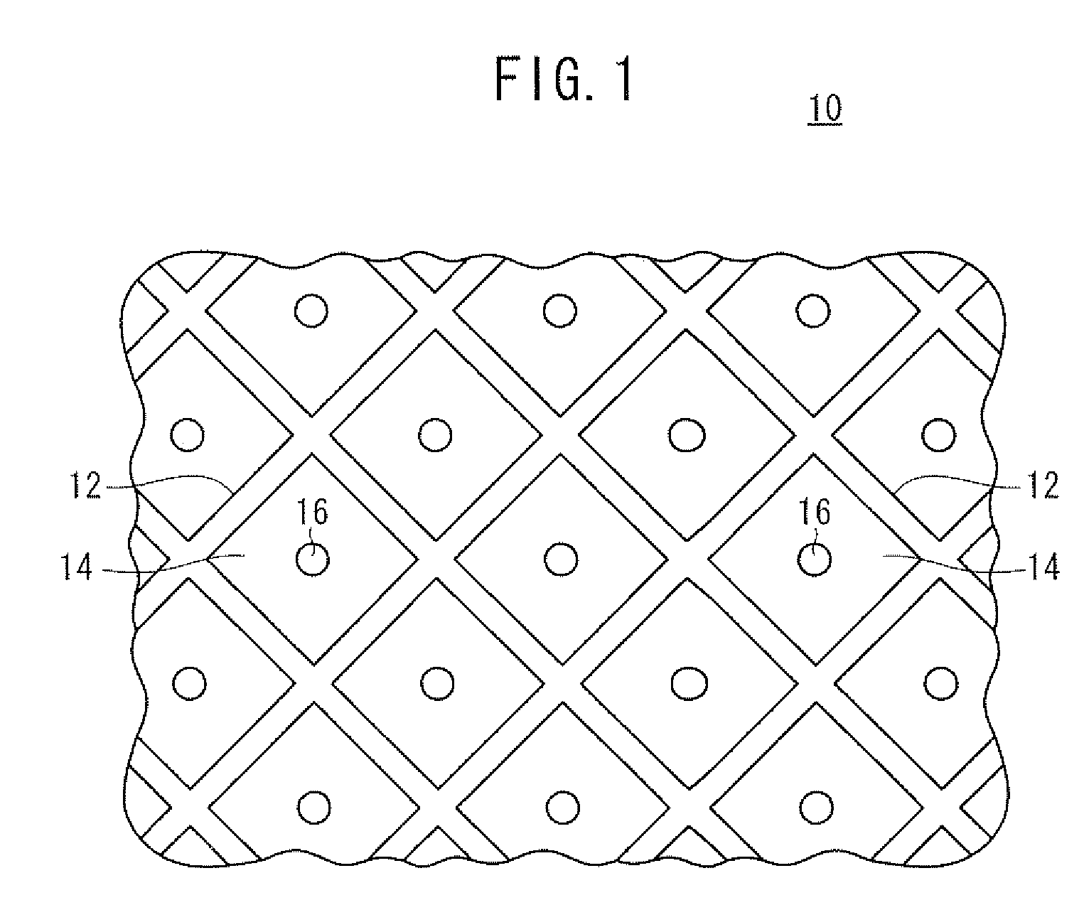
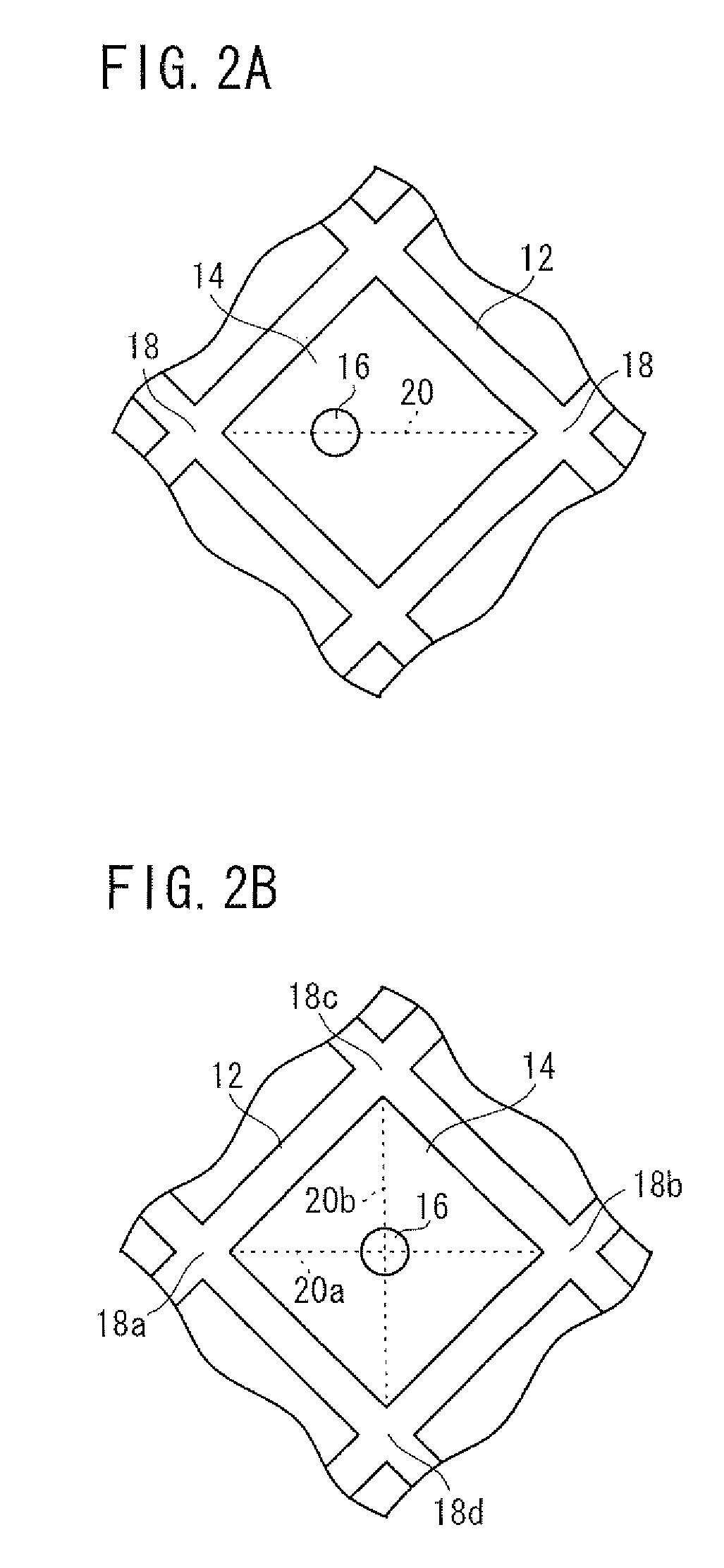
[0324]As shown in Table 2, in Examples 1 to 7, the conductive portion 12 of the mesh pattern 32 had a wire width of 14 μm, and the moire preventing part 16 was formed at the center of the opening portion 14. The ratios (Sb / Sa) of the area Sb of the intersection 18 to the area Sa of the moire preventing part 16 were 0.1, 0.5, 0.9, 1.0, 1.1, 1.5, and 1.9, respectively.

[0325]In Examples 8 to 14, the conductive portion 12 of the mesh pattern 32 had a wire width of 21 μm, and the moire preventing part 16 was formed at the center of the opening portion 14. The ratios (Sb / Sa) of the area Sb of the intersection 18 to the area Sa of the moire preventing part 16 were 0.1, 0.5, 0.9, 1.0, 1.1, 1.5, and 1.9, respectively.

[0326]In Examples 15 to 21, the conductive portion 12 of the mesh pattern 32 had a wire width of 28 μm, and the moire preventing part 16 was formed at the center of the opening portion 14. The ratios (Sb / Sa) of the area Sb of the intersection 18 to the area Sa of the moire preve...


PUM


Abstract

An electromagnetic shielding film comprises a conductive portion and an opening portion, and a moire preventing part is formed in the opening portion. The moire preventing part may be formed approximately at the center of the opening portion, and may be formed on a line connecting intersections facing each other in the conductive portion in the mesh pattern. The moire preventing part may have a substantially circular planar shape or a polygonal planar shape (such as a quadrangular, pentagonal, hexagonal, or octagonal shape). Of course the moire preventing part may have an at least partially curved planar shape. The electromagnetic shielding film preferably satisfies the inequality 0.1Sa≦Sb≦5.0Sa, in which Sa is the area of the intersection of the conductive portion and Sb is the area of the moire preventing part.

Description

BACKGROUND OF THE INVENTION[0001]1. Field of the Invention[0002]The present invention relates to an electromagnetic shielding film and an optical filter, particularly to an electromagnetic shielding film and an optical filter that are light transmittable and capable of shielding electromagnetic waves from front surfaces of display devices such as CRTs (cathode ray tubes), PDPs (plasma display panels), liquid crystal displays, EL (electroluminescence) displays, and FEDs (field emission displays), microwave ovens, electronic devices, printed circuit boards, and the like.[0003]2. Description of the Related Art[0004]Problems of electro-magnetic interference (EMI) have been rapidly increasing in recent years along with increase in the use of various electric and applied-electronic equipments. It has been indicated that the EMI causes malfunction or failure of the electronic or electric equipment, and further causes health disorder of an operator of the equipment. Therefore, the electroni...

Claims


Application Information

Patent Timeline
Patent Type & Authority Applications(United States)
IPC IPC(8): H05K9/00
CPCH05K9/0096G02F2001/133334G02F1/133334
Inventor SANETO, RYUJISEKIGUCHI, MEGUMIISHIZUKA, HIROSHI
Owner FUJIFILM CORP
Why Eureka
Try Eureka