Multilayer structural body and method for cleaning the same

a multi-layer structure and cleaning technology, applied in the direction of superimposed coating process, cleaning using liquids, transportation and packaging, etc., can solve the problems of unavoidable shrinkage during baking, unavoidable increase in size of various ceramic members used in semiconductor manufacturing apparatuses, and failure of circuits, etc., to achieve rapid and economical adjustment, increase in the size of a structural member, and high cleaning

Inactive Publication Date: 2009-05-28
TOHOKU UNIV +1
View PDF18 Cites 22 Cited by
  • Summary
  • Abstract
  • Description
  • Claims
  • Application Information

AI Technical Summary

Benefits of technology

[0034]According to this invention, by providing a laminated structural body having a ceramic layer at its surface, there is an effect that it is possible to quickly and economically cope with an increase in size of a structural member. Further, since high-cleanness cleaning can be performed for the ceramic layer deposited on a base member, high cleanness can be maintained. Further, since the adhesion strength of the deposited ceramic layer is high, even if an ultrasonic wave of 5 W / cm2 or more and 30 W / cm2 or less is applied in the high-cleanness cleaning, there is no occurrence of stripping or the like.

Problems solved by technology

If a wafer or a liquid crystal panel is brought into direct contact with such a member with the contaminants remaining thereon, the contaminants are accumulated on the surface of the wafer or the liquid crystal panel to cause a circuit failure.
As described above, along with the increase in size of semiconductor manufacturing apparatuses, various ceramic members for use in those semiconductor manufacturing apparatuses unavoidably increase in size.
However, since a ceramic member is manufactured by baking at a high temperature of 1000° C. or more, shrinkage unavoidably occurs during the baking.
As a result, it becomes more difficult to achieve dimensional accuracy as the ceramic member increases in size.
Further, as the ceramic member increases in size, the baking is required for a longer time.
Therefore, it is difficult to manufacture a ceramic member that is large in size and still has precise dimensions, in a short time and economically.
Therefore, the current situation is that it is practically difficult to quickly respond to the requirement for increase in size using a ceramic member alone.Patent Document 1: Japanese Unexamined Patent Application Publication (JP-A) No. 2004-279481Patent Document 2: Japanese Unexamined Patent Application Publication (JP-A) No.

Method used


Image

  • Multilayer structural body and method for cleaning the same
  • Multilayer structural body and method for cleaning the same
  • Multilayer structural body and method for cleaning the same

Examples


first embodiment

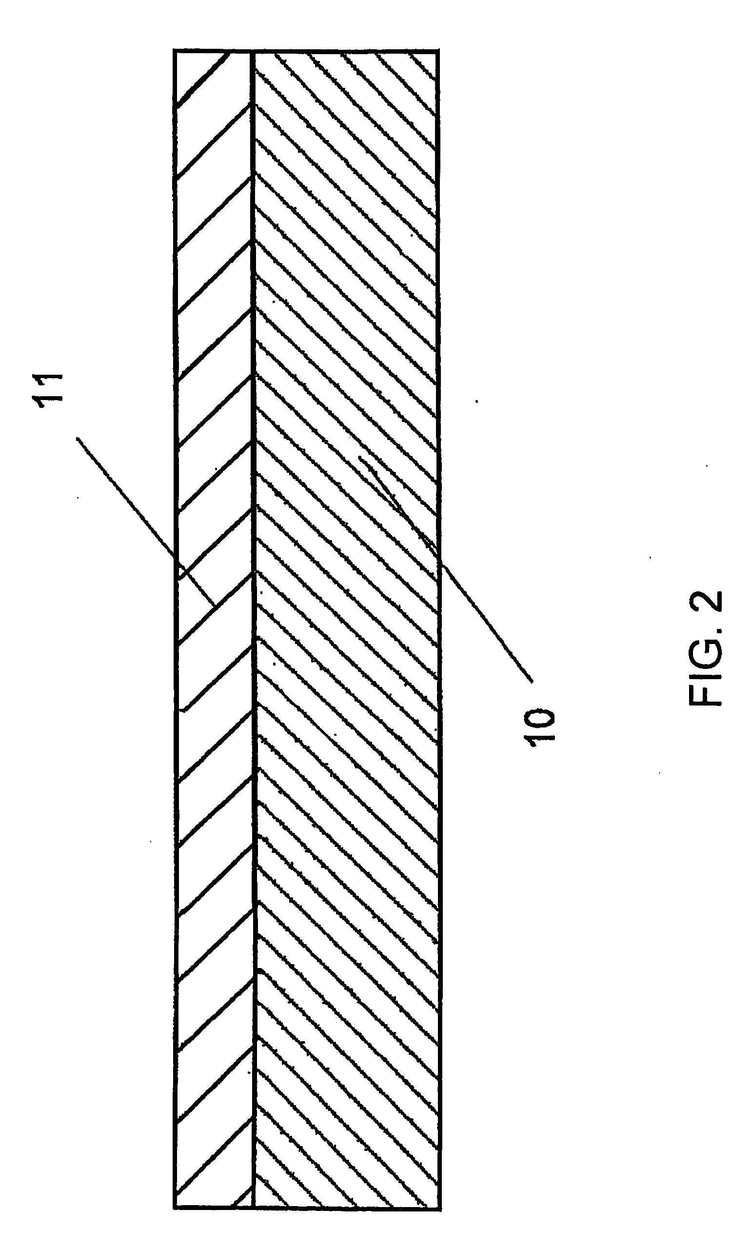
[0053]Referring to FIG. 2, a multilayer structural body according to this invention comprises, for example, a base member 10 and a ceramic layer 11 in the form of yttria deposited by plasma spraying (i.e. a plasma-sprayed Y2O3 layer) on the surface of the base member. Herein, an aluminum alloy with a diameter of 40 mm and a thickness of 3 mm is used as the base member 10 and the plasma-sprayed film is formed as the ceramic layer 11 on the surface of the base member 10. The illustrated plasma-sprayed film is the Y2O3 layer having a thickness of 200 μm. A spray apparatus described, for example, in Patent Document 2 or Patent Document 3 can be used for the plasma spraying.

[0054]A ceramic film is preferably Y2O3, Al2O3, MgO, or a compound thereof for a semiconductor manufacturing apparatus in terms of plasma resistance.

[0055]In the illustrated example, the ceramic layer 11 is directly formed on the surface of the aluminum alloy base member 10. However, the surface of the aluminum alloy ...

second embodiment

[0063]Referring to FIG. 4, a multilayer structural body according to this invention will be described. The multilayer structural body according to this embodiment is formed using an atmosphere-open thermal CVD apparatus shown in FIG. 4. This CVD apparatus comprises a flowmeter 21, an evaporator 23, and a nozzle 25, wherein a silicon wafer forming a base member 10 is placed on a heater 27 and the illustrated silicon wafer has a diameter of 200 mm. As illustrated, the evaporator 23 and the nozzle 25 are covered by a heater 29.

[0064]An organic metal complex containing Y is stored as a material in the evaporator 23 where a nitrogen gas (N2) is introduced through the flowmeter 21 and this material is evaporated by heating and introduced onto the base member 10 through the nozzle 25. As a result, a Y2O3 film is deposited as a deposited film on the silicon wafer forming the base member 10. It has been found that this deposited film exhibits an adhesion strength higher than that of the plas...

third embodiment

[0067]Next, referring to FIGS. 6(a) and (b), a multilayer structural body according to this invention will be described. The multilayer structural body is obtained by first coating a ceramic precursor 33 on a base member 10 using a spray gun 31 as shown in FIG. 6(a) and then baking them in an oven 35. By baking the precursor 33, formed by the spray gun 31, at a temperature of about 300° C. in the oven 35, there is obtained a high-purity, high-density ceramic film, for example, a Y2O3 film. The technique of forming the Y2O3 film in this manner is called herein a sol-gel method.

[0068]According to this method, it is possible to easily form a high-purity ceramic film at a relatively low temperature. Actually, when a Y2O3 film was formed on an aluminum base member 10, there was obtained the Y2O3 film having Ra of 0.11 μm when the base member 10 had Ra of 0.18 μm.

[0069]In the foregoing example, the description has been given of the case where the precursor is coated by the spray gun 31. H...


PUM

PropertyMeasurementUnit
particle sizeaaaaaaaaaa
temperatureaaaaaaaaaa
thicknessaaaaaaaaaa

Abstract

It has been difficult to provide a large-sized ceramic member quickly and economically. A multilayer structure is produced by forming a ceramic film on a base which is made of a material that can be shaped comparatively easily. The ceramic film is formed by a plasma spraying method, CVD method, PVD method, sol-gel method or the like. Alternatively, the ceramic film may be formed by a method combined with a spray deposit film.

Description

TECHNICAL FIELD[0001]This invention relates to a structural body used as a component or a member for use in an environment where high cleanness is required, such as in the dry process for electronic devices, the manufacture of medical supplies, or the processing / manufacture of foodstuffs, and to a cleaning method therefor.BACKGROUND ART[0002]The miniaturization of the design rule of semiconductors has been advanced following the improvement in integration thereof and thus it has been required to reduce the allowable size and amount of adhering substance and metal contaminants. Further, in terms of sanitation of medical supplies, foodstuffs, and so on, it is required to reduce adhering substance and metal contaminants. Normally, structural bodies that hate metal contaminants or the like employ ceramics as members thereof. Particularly, structural bodies forming semiconductor and liquid-crystal manufacturing apparatuses tend to increase in size following the increase in size of wafers...

Claims


Application Information

Patent Timeline
Patent Type & Authority Applications(United States)
IPC IPC(8): B08B3/12B32B5/16
CPCB08B3/02B08B3/12B08B2203/0288C23C4/00C23C4/02Y10T428/25C23C16/405C23C16/545C23C26/00C23C28/04Y10T428/252C23C4/105C23C4/11H01L21/205H01L21/3065
Inventor OHMI, TADAHIROTERAMOTO, AKINOBUMORINAGA, HITOSHIKISHI, YUKIOOHTAKI, HIROMICHITSUTAI, YOSHIHUMI
Owner TOHOKU UNIV
Why Eureka
Try Eureka