Test circuits and current pulse generator for simulating an electostatic discharge

a current pulse generator and test circuit technology, applied in electrical testing, measurement devices, instruments, etc., can solve the problems of inability to connect the iec test specified esd pulse generator to the typical ic device, difficult to test a cut with tools and methods designed for eut, and inability to directly apply to testing of subassemblies, etc., to achieve the effect of reducing effectively attenuating the generated em puls

Inactive Publication Date: 2009-05-28
GRUND EVAN
View PDF8 Cites 54 Cited by
  • Summary
  • Abstract
  • Description
  • Claims
  • Application Information

AI Technical Summary

Benefits of technology

[0017]An advantage of using controlled impedance delivery cables is that the current pulses are transmitted with little distortion, allowing fast pulse rise times to be delivered over a distance of several meters from the pulse generator to the CUT. Without the use of controlled impedances the parasitic wiring capacitances and / or inductances will attenuate the high frequencies of the current pulse causing the pulse to be modified as it is transmitted. Using delivery cables allows flexibility in applying ESD testing to a wide physical variety of CUT types.
[0018]CUTs, such as IC devices, can be in different physical forms, therefore, flexibility in connecting ESD testers to CUTs is an important feature of this invention. For example, if an IC is still in wafer form, as manufactured before being cut into individual dice, a wafer probing system featuring 50-ohm wafer probes may be used as a means of interfacing the pulse to the CUT. Wafer probes are also compatible with packaged CUTs and modules, as well as board assemblies and other component configurations.
[0020]The production and delivery of current waveforms defined in the IEC Test specification is an application of the present invention. It is a purpose of this invention to remove problems of prior art IEC Test pulse generators. This invention makes improvements over prior art that will be described hereinafter, including: preventing strong EM pulses from impinging on the CUT and causing testing variations, generating pulses with high reproducibility, providing CUT current monitoring that can measure stress level and detect changes in CUT impedance, making testing easy due to integrated leakage measurement and automating test sequences and automatic report generation.
[0027]The IEC Test describes a testing table with horizontal and vertical metallic coupling planes upon which the equipment under test (EUT) is placed. Waveform variations with the IEC Test discharge gun are observed in different testing environments due to the gun's EM pulse that interacts with such coupling planes. An EM pulse is generated from the rapid change in current that occurs in an ESD simulator during pulse generation. Some prior art gun pulse generators purposely produce additional EM pulse radiation as part of their waveform shaping methods. A purpose of the delivery cable is to allow separation between the pulse source that will generate an EM pulse, and the CUT. The distance of separation can be large enough to effectively attenuate the generated EM pulse to a negligible level. EM pulses are attenuated by the square of the distance between the pulse source and CUT. Adding a meter of cable can reduce the EM pulse to only 3% of the strength from a gun discharge. It is a purpose of the present invention to not require special testing environments such as metallic covered tables or coupling planes.

Problems solved by technology

This testing method was designed only for testing complete systems, and is not directly applicable to testing of subassemblies, such as circuit boards, or of individual IC components or devices, often collectively termed a component under test (CUT).
Testing a CUT with tools and methods designed for an EUT is difficult.
A primary reason for difficulty in applying the IEC Test to circuit boards or IC devices is the inability of the IEC Test specified ESD pulse generator to be connected to the typical IC device.
Such prior art ESD pulse generators using a metallic probe tip are difficult to connect to the small dimensions of today's microelectronic circuitry.
Gun testing is especially difficult with high density packaging of modern ICs, which may have pin-to-pin spacing of 0.5 millimeters or less.
Improper connection leads to pulse distortions that can adversely affect the testing results.
Connection from the IEC Test discharge gun to a CUT has been attempted in a variety of ways, and often with inconsistent results.
These unwanted EM radiation pulses complicate the testing environment, and EM pulse shielding is sometimes done to help mitigate the effect.
Given these factors, a good deal of uncertainty can be introduced into IC test results when using IEC Testing discharge guns.
This approach suffers from pulse shape distortion due to different electrical properties of the gun and the TFB.
The wiring of TFBs can have impedances from about 30 to 150 ohms, but cannot be manufactured at 330 ohms due to physical printed wiring size limits.
The mismatch of impedances will result in pulse reflections and waveform distortions to the fast current pulses.
Such prior art testing also suffers from non-reproducibility due to TFB-to-TFB design variations in the conductive paths to the CUT.
With the miniature contacts on small microelectronic components, this can be very difficult.
Even when more than one robot is used it can be impossible to make contacts to neighboring pins due to the size of the IEC Test gun's metallic tip.
However, the IEC Test requires many amperes of current and hundreds, or even thousands, of volts to reach desired stress testing levels.
These requirements for high power levels are far beyond the capabilities of common arbitrary waveform generators.
Prior art test methods lack the power, reproducibly and consistency in applying stress pulses to ICs or other devices that is needed for repeatability in testing.

Method used


Image

  • Test circuits and current pulse generator for simulating an electostatic discharge
  • Test circuits and current pulse generator for simulating an electostatic discharge
  • Test circuits and current pulse generator for simulating an electostatic discharge

Examples


Embodiment Construction

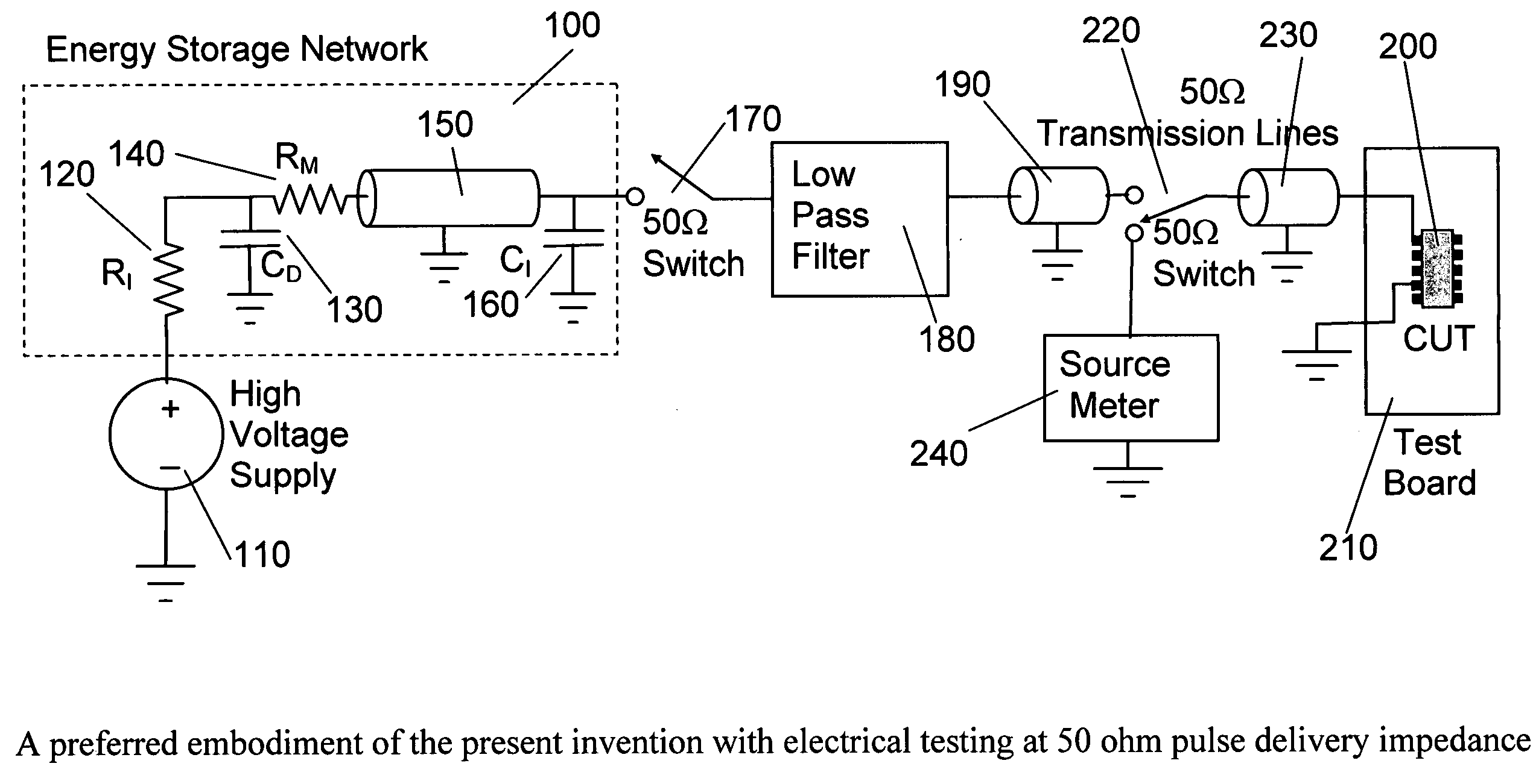
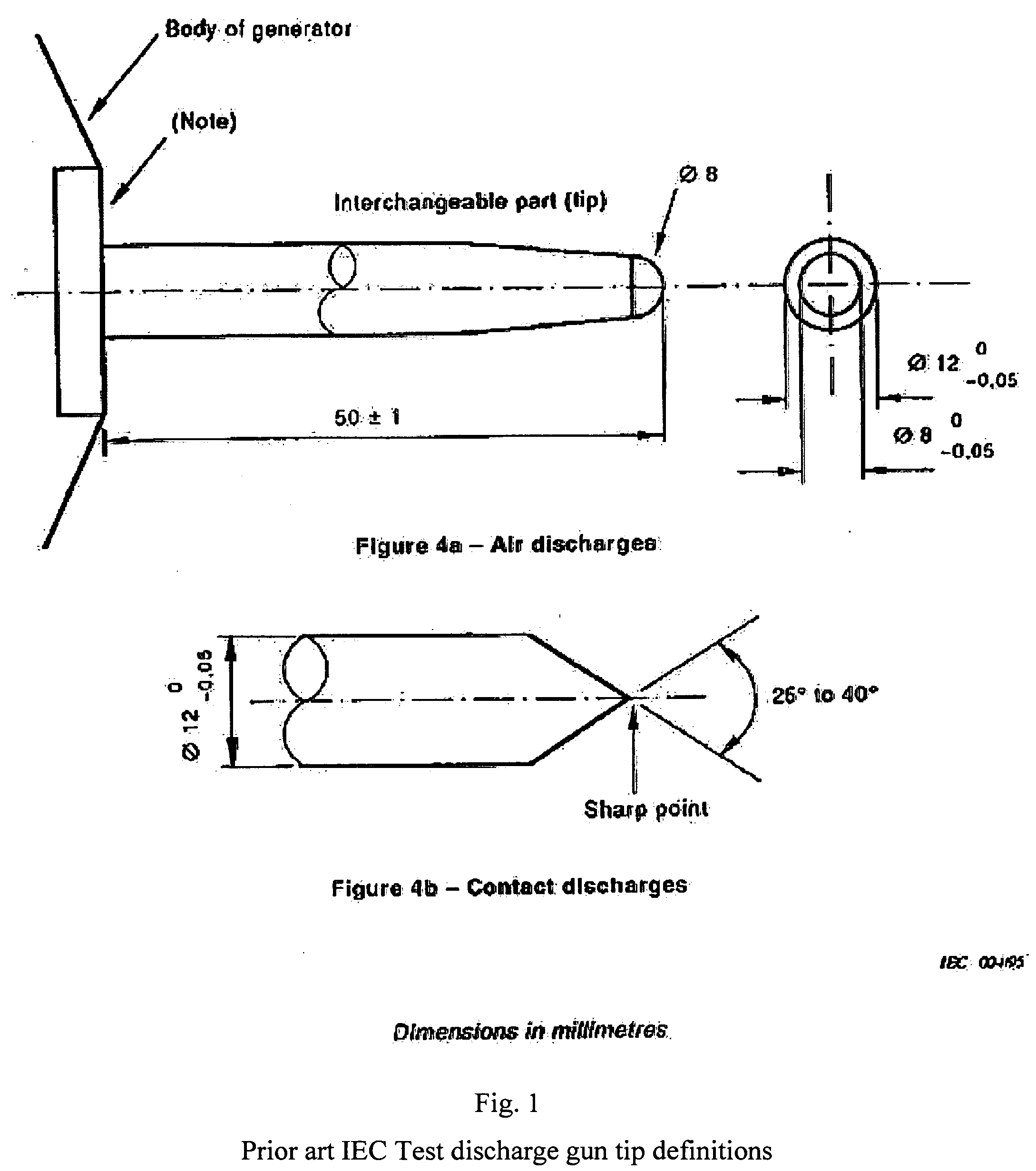
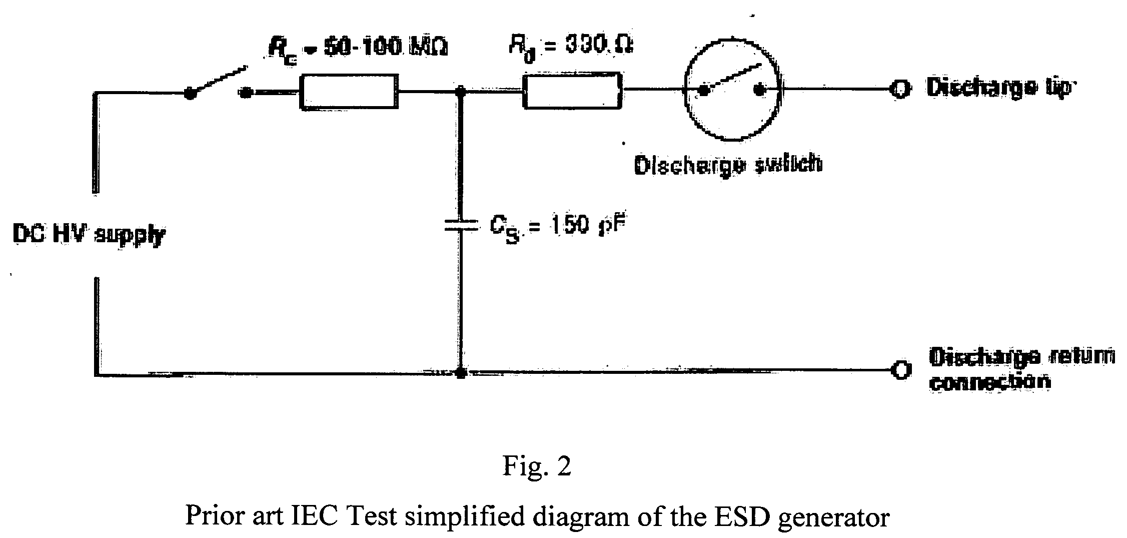
[0037]In the following description, numerous specific details are provided, such as the identification of various system components, to provide a thorough understanding of embodiments of the invention. One skilled in the art will recognize, however, that the invention can be practiced without one or more of the specific details, or with other methods, components, materials, etc. In still other instances, well-known structures, materials, or operations are not shown or described in detail to avoid obscuring aspects of various embodiments of the invention. Reference throughout this specification to “one embodiment” or “an embodiment” means that a particular feature, structure, or characteristic described in connection with the embodiment is included in at least one embodiment of the present invention. Thus, the appearance of the phrases “in one embodiment” or “in an embodiment” in various places throughout this specification are not necessarily all referring to the same embodiment. Fu...


PUM


Abstract

This invention is an electrostatic discharge testing circuit that can deliver current pulses to a component under test (CUT) with a custom amplitude versus time profile shape. Pulse generation with customized shapes is accomplished by discharging an energy storage network comprised of capacitor(s), transmission line(s) and other passive components. Current pulses compliant to the European International Electrotechnical Commission IEC 61000-4-2 standard can be so produced. These current pulses are delivered to the CUT with low distortion through a constant impedance electrical path, such as a combination of cables and controlled impedance conductors of printed wiring boards compatible with packaged IC devices, assemblies, and wafer probes. The current pulses can be delivered with various impedances, and measurements made that allow the CUT currents and voltages to be calculated.

Description

CROSS REFERENCE TO RELATED APPLICATION[0001]This application claims the benefit of U.S. Provisional Application No. 61 / 003,908, filed Nov. 23, 2007, which is incorporated herein by reference.BACKGROUND OF THE INVENTION[0002]1. Field of the Invention[0003]The present invention relates generally to electrical testing circuitry for integrated circuits (ICs) and in particular to apparatus for electrostatic discharge (ESD) sensitivity testing that includes a pulse generator (pulser).[0004]2. Description of the Related Art[0005]Testing of ICs for ESD sensitivity involves applying stress pulses simulating electrostatic discharges to an IC or device under test to determine robustness. The use of this stress testing is expanding to help ensure reliability of products such as computers and cell phones when they are exposed to ESD. Equipment that must operate in harsh and / or high static environments, such as automotive electronics, also requires thorough ESD reliability testing.[0006]All elect...

Claims


Application Information

Patent Timeline
Patent Type & Authority Applications(United States)
IPC IPC(8): G01R31/02
CPCG01R31/2841G01R31/002
Inventor GRUND, EVAN
Owner GRUND EVAN
Why Eureka
Try Eureka