Method to improve the write speed for memory products

a technology of memory products and write speeds, applied in the field of memory integrated circuits, can solve the problems of potential difference between bit-lines, power consumption increase, and difficulty in detecting voltage differences between complementary voltage levels on a pair of bit-lines, and achieve good write stability, high write speed, and good write stability

Inactive Publication Date: 2009-06-11
ETRON TECH INC
View PDF5 Cites 18 Cited by
  • Summary
  • Abstract
  • Description
  • Claims
  • Application Information

AI Technical Summary

Benefits of technology

[0029]Also in accordance with the objects of this invention a new method is described, capable of implementing a Random Access Memory (RAM) product with Data-Line Bit Switch pass transistors implemented as thick-oxide MOS transistor components and realized as an Integrated Circuit (IC) fabricated in CMOS technology, comprising: providing a means for realizing the function of a Bit-Line Sense Amplifier (BLSA) which consists of an amplifying means built with MOS transistors of the PMOS and/or NMOS type, here all together designated as BLSA-transistors; providing a pair of Bit Switch (BS) pass transistors implemented as thick-oxide MOS transistors operating as FET-switches and gate controlled by a BS control signal with maximum voltage VBS thus forming two thick-oxide MOS-transistors named as BS FET-switches; providing a pair of Data-Line (DL) conductors connected to one side of said pair of Bit Switch (BS) pass transistors named as BS FET-switches, which on their other side are connected to certain connection points of said means for realizing the function of a Bit-Line Sense Amplifier (BLSA) and serving as input/output terminal pins therefore feeding a first line with normal potential and a second line with complementary potential together forming a pair of complementary Data-Lines switched by said pair of MOS transistors named as BS FET-switches; connecting said input/output terminal pins of said means for realizing the function of a Bit-Line Sense Amplifier (BLSA) to the drains/sources of said pair of Bit Switch (BS) MOS transistors named as BS FET-switches; connecting the sources/drains of said pair of Bit Switch (BS) MOS transistors named as BS FET-switches to said pair of complementary Data-Lines; realizing said RAM product as an IC fabricated in CMOS technology introducing two thicknesses for oxide layers added to a standard CMOS process in order to produce said thin and thick-oxide MOS transistors; implementing said MOS BLSA-transistors within said means for realizing the function of a Bit-Line Sense Amplifier (BLSA) as thin-oxide MOS transistors with maximum gate voltage VCC, the core voltage of the device e.g.; dimensioning the gates of said MOS BLSA-transistors made as thin-oxide MOS transistors within said Bit-Line Sense Amplifier by its Width-to-Length ratio (W/L)12=Y12; implementing said pair of Bit Switch (BS) MOS transistors as thick-oxide MOS transistors with maximum gate voltage VPP, a charge pump voltage of the device e.g. which is greater as VCC, i.e. VPP>VCC; dimensioning the gates of said MOS transistors made as thick-oxide MOS transistors for said Bit Switch transistors by its Width-to-Length ratio (W/L)34=Y34; choosing the gate dimension (W/L)34=Y34 of said thick-oxide MOS transistors much smaller than the gate dimension (W/L)12=Y12 of said thin-oxide MOS transistors; choosing said maximum voltage value VBS of said Bit Switch control signal driving the gate of said Bit Switch transistors as high as said maximum gate voltage VPP; and optimizing said maximum voltage value VBS of said Bit Switch control signal within said RAM IC for both, a good write stability and a high write speed.
[0030]Finally in accordance with the objects of this invention a new method is described, capable of implementing a Bit-Line Sense Amplifier with Data-Line Bit Switch pass transistors for Ra

Problems solved by technology

As the density of semiconductor memory devices increases, simultaneously the operating power supply voltages decrease thereby also reducing current and consequently also alleviating power consumption.
Due to the trend in decreasing power-supply voltages for semiconductor memory devices, it is difficult to sense the voltage difference between complementary voltage levels on a pair of Bit-Lines, even with specialized voltage type Sense Amplifiers.
As a result, charges in the capacitor within each Unit Memory Cell are transferred onto the Bit-Lines causing a potential difference between the Bit-Lines.
However, because of the relatively small potential change between the Bit-Lines, the amplifying process would be much less stable and unreliable.
However, as a practical matter, the storage capacitor discharges over the course of time via the access transistor and its dielectric layer thereby losing th

Method used


Image

  • Method to improve the write speed for memory products
  • Method to improve the write speed for memory products
  • Method to improve the write speed for memory products

Examples


Embodiment Construction

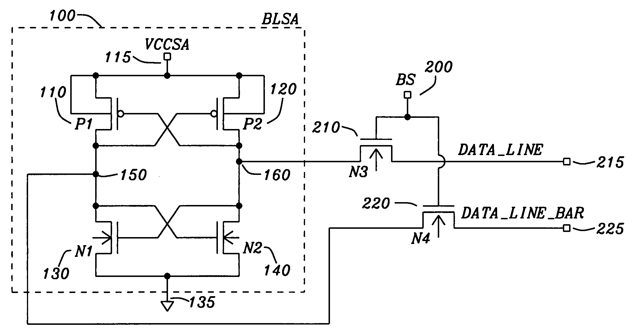
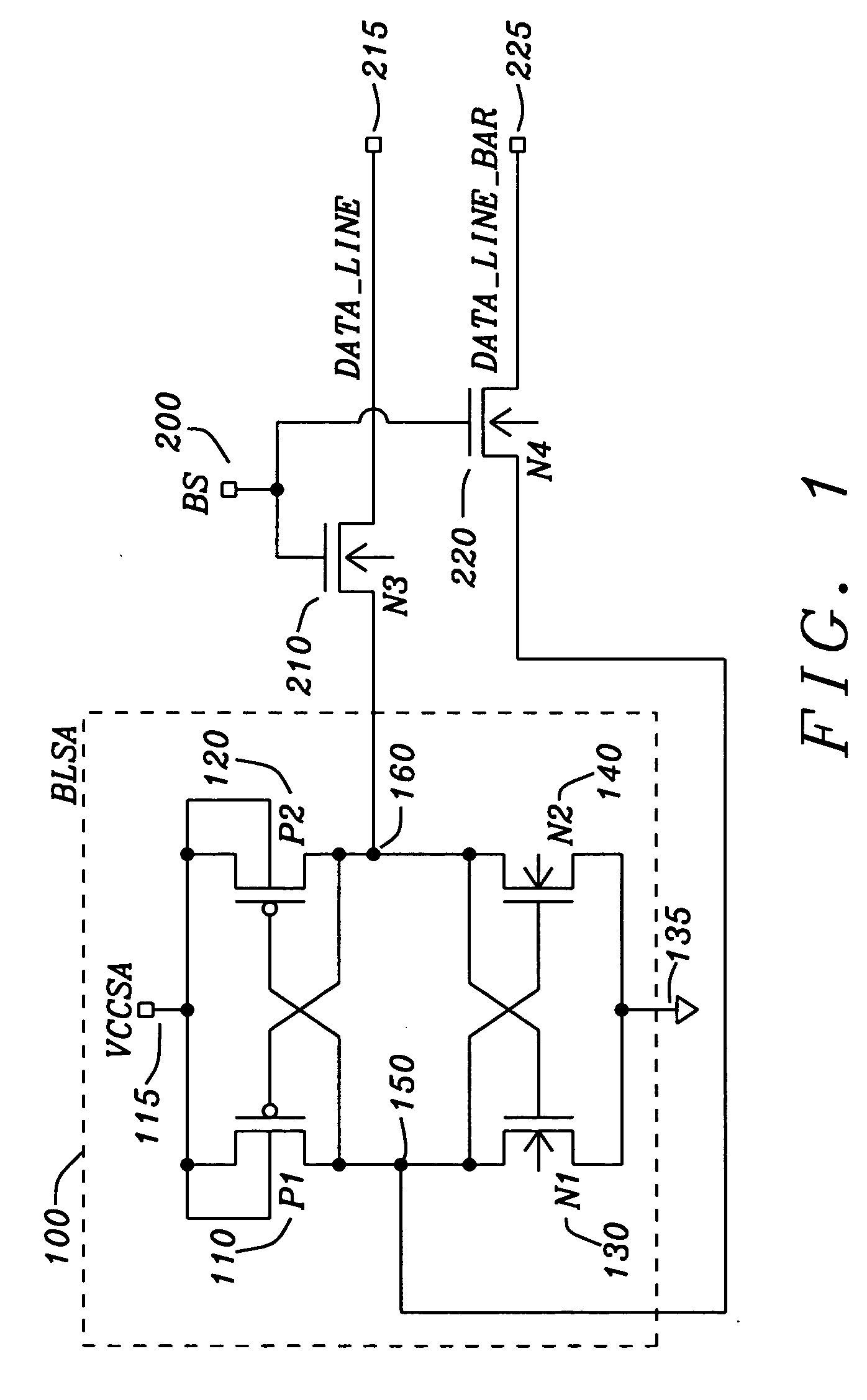
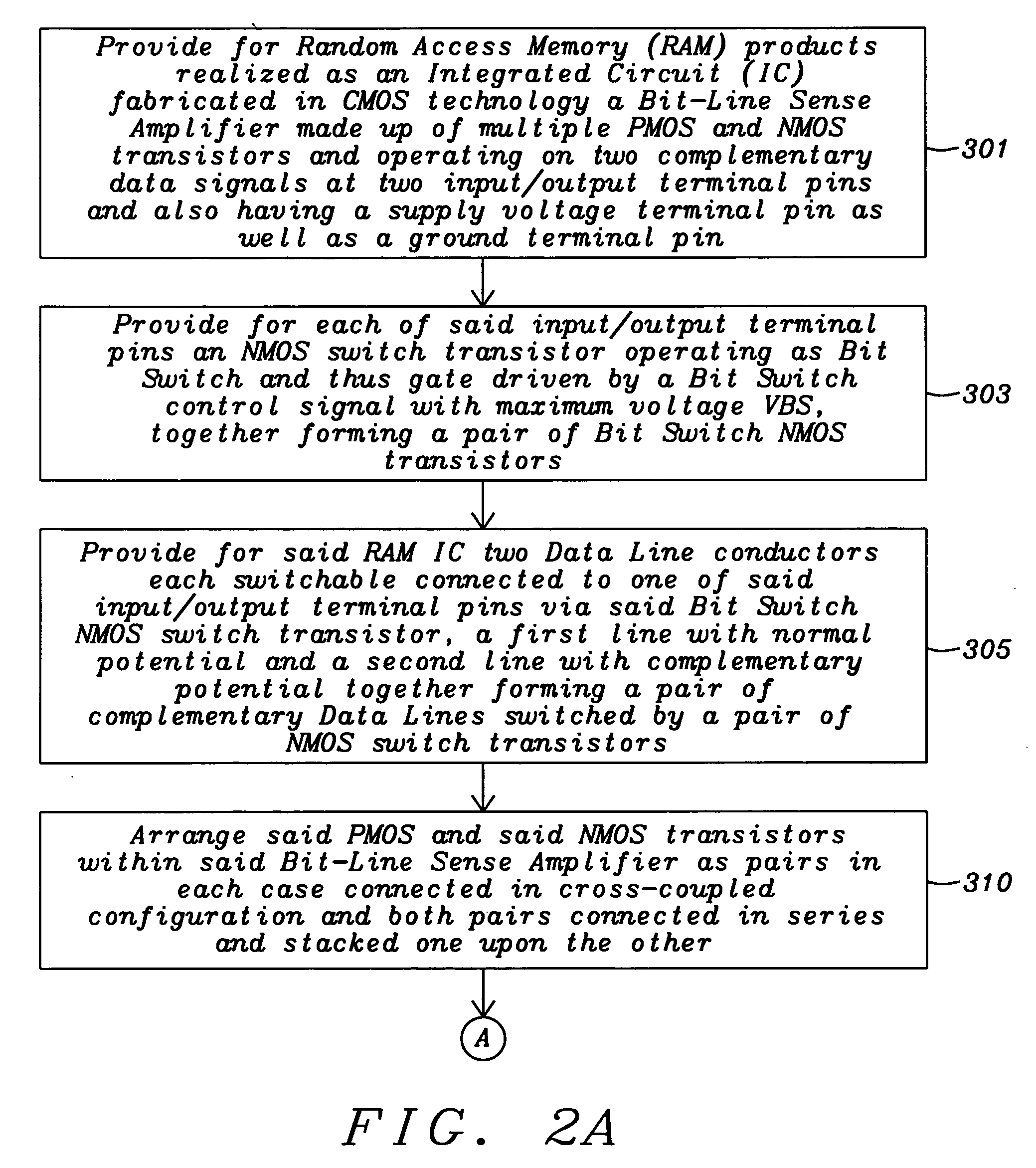
[0034]The preferred embodiment discloses a novel realization for a “Bit-Line Sense Amplifier with Bit Switch” circuit for semiconductor memory ICs. The technical approach for achieving the goal of sped-up Write operations for integrated memory circuit in DRAM configuration uses a two thickness technique of oxide layers for realizing crucial internal auxiliary circuit parts of the chip. Using the intrinsic advantages of that solution—as described later on in every detail—the method for using the circuit of the invention as realized with standard CMOS technology at low cost is described.

[0035]Contemplating now FIG. 1, a circuit diagram of the new realization for the “Bit-Line Sense Amplifier with Bit Switch” circuit of this invention for memory devices is depicted. As can be seen from the schematics a Bit-Line Sense Amplifier block (item 100) abbreviated as BLSA delivers two complementary signals named DATA_LINE (215) and DATA_LINE_BAR (225) respectively controlled by two Bit-Line Swi...


PUM


Abstract

A method and circuit are given, to realize a Bit-Line Sense Amplifier with Data-Line Bit Switch (BS) pass transistors for Random Access Memory (RAM) products as Integrated Circuit (IC) fabricated in CMOS technology with optimized operating characteristics of said RAM product with respect to good write stability and high write speed and wherein the layout area of the BS FET-switches and thus also the die size is minimized. This is achieved by using a two thickness technique of oxide layers for crucial internal circuit parts of the chip.

Description

BACKGROUND OF THE INVENTION[0001](1) Field of the Invention[0002]The present invention relates in general to semiconductor design technology; more particularly this invention relates to the manufacture of memory Integrated Circuits (IC), and even more particularly to a semiconductor memory IC having an optimized chip area design with enhanced writing speed behavior via technologically adapted data-line selection devices in such memory circuits.[0003](2) Description of the Related Art[0004]In general, electronic data storage devices built as integrated memory circuits are made up of a large number of memory cells arranged in the form of a matrix or array with rows and columns. These arrays are surrounded by a number of auxiliary elements —also called peripheral circuits—necessary for achieving the purpose of those data storage operations, i.e. writing data into and accordingly reading data from addressed memory cells within that storage device, all this under control of read / write en...

Claims


Application Information

Patent Timeline
IPC IPC(8): G11C7/06
CPCG11C7/065G11C2207/002G11C7/1006
Inventor SHIAH, CHUN
Owner ETRON TECH INC
Why Eureka
Try Eureka